
Adder circuit
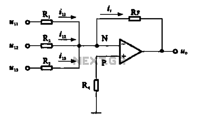
The inverting adder circuit operates based on the principle of superposition. Each input voltage is applied through its respective resistor to the inverting terminal of the operational amplifier. The output voltage (V_out) can be expressed mathematically as V_out = - (R_f/R_i) * (V_1 + V_2 + V_3 + ... + V_n), where R_f is the feedback resistor and R_i represents the input resistors corresponding to each input voltage. The negative sign indicates that the output is inverted relative to the input signals.
In the typical configuration, the operational amplifier's inverting input is connected to the junction of the input resistors. The feedback resistor R_f connects from the output back to the inverting input, creating a feedback loop essential for the operation of the amplifier. The non-inverting input is typically grounded or connected to a reference voltage, ensuring stability in the circuit.
The balancing resistor R4 plays a critical role in maintaining the correct gain and stability of the circuit. Its value is chosen to match the equivalent resistance of the input resistors to minimize offset errors and ensure accurate summation of the input signals. The design allows for flexible scaling of the output voltage by adjusting the feedback and input resistors, thus enabling the circuit to accommodate a variety of applications, such as audio mixing, signal processing, and data acquisition systems.
Overall, the inverting adder circuit is a fundamental building block in analog electronics, providing a straightforward method for summing multiple voltage signals while maintaining control over the gain and phase characteristics.Adder circuit commonly used inverting input, namely the inverting adder circuit. It was to the inverting input of the operational amplifier electrical path, based on the signal voltage to be added through a resistor connected to the inverting input terminal of the operational amplifier. Adder circuit shown in Figure 7-5, which is having a three input inverting adder circuit. Wherein the input signal number eight ii, machine 2,1113 are N input from the inverting input terminal, pin feedback resistors, non-inverting input terminal P via the balancing resistor R4 connected to.
The resistance value of the balancing resistor R4 vase should be Ri, R2, R3 and the parallel and Rr. The output voltage of adder circuit input voltage is equal to the sum of the branch, which kind of structure can be realized adder plurality of input signals.
Related Circuits
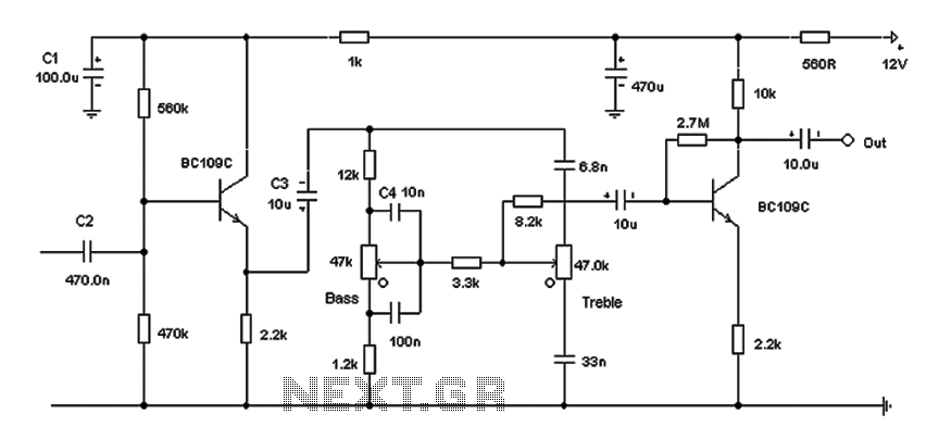
Based on the classic Baxendall tone control circuit, this design offers a maximum cut and boost of approximately 10 dB at 10 kHz and 50 Hz. Since the controls are passive, the final transistor provides a slight boost. The...
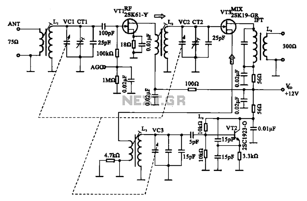
The FM radio circuit consists of a high-frequency amplifier (VT1), a mixer and local oscillator (VT2), and additional components. The circuit includes an FM radio antenna for signal detection, with an input transformer (L1) connected to a gate transistor...
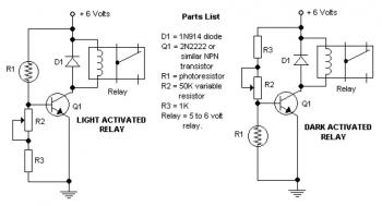
The potentiometer adjusts the trigger level. The diode in the circuit diagram is specified as 1N914, which is suitable for light-duty relays; however, since the 1N914 is a signal diode, it is not ideal for this application. A 1N4001...

This is a simple circuit design for a video transmitter capable of radiating signals up to 50 meters. The video transmitter can be connected to a camera as a source and allows viewing on a VHF channel analog television....
The individual is new to electronics but enjoys experimentation. They plan to create a small guitar amplifier based on a 30 Watt design, specifically the single 12VDC version referenced in comments. The intention is to incorporate a preamplifier to...
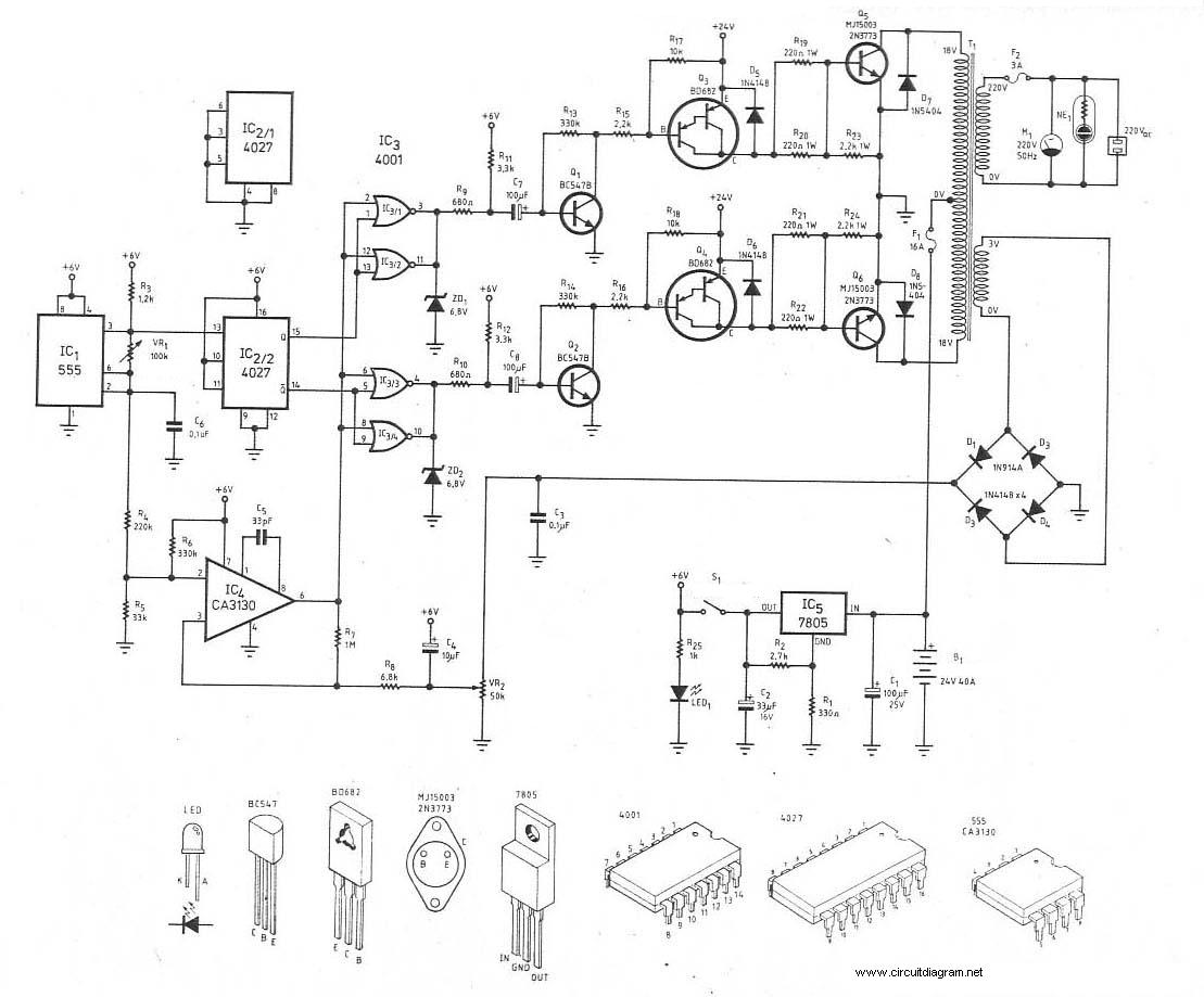
This is the schematic diagram of a 300W power inverter circuit. The inverter utilizes the MJ15003 power transistor for final amplification. If the MJ15003 transistor is difficult to source, it can be replaced with a 2N3773. The inverter is...