
parallel inverter

The parallel inverter circuit is essential for reliable power conversion in UPS applications. The two SCRs (T1 and T2) serve as controlled switches that manage the flow of current through the transformer, enabling the inverter to produce a stable AC output from a DC input. The inductor (L) plays a pivotal role in maintaining a steady current flow, which is critical for the consistent operation of the inverter. The commutating capacitor (C) facilitates the switching action between the SCRs, allowing for efficient energy transfer and maintaining the desired voltage levels across the load.
In operation, the inverter alternates between the two SCRs to create a square wave output voltage. The timing of the triggering pulses to the gates of T1 and T2 is crucial, as it determines the frequency and waveform of the output voltage. The transformer provides isolation and voltage step-up as required, while the inductor ensures that the current remains stable during the switching transitions. The overall design must account for the ratings of the components, including the voltage and current handling capabilities of the SCRs, the inductance value, and the capacitance of the commutating capacitor, to ensure reliable and efficient operation.
In summary, the parallel inverter circuit is a sophisticated arrangement that effectively converts DC to AC, ensuring uninterrupted power supply to critical loads. Its operation relies on the coordinated switching of SCRs, the stability provided by the inductor, and the timely charging and discharging of the capacitor, all of which contribute to the inverter's performance and reliability in various applications.The inverter plays a vital role in Uninterrupted Power Supply (UPS). It is used to convert the direct current (DC) to alternating Current (AC) of required voltage. The basic single phase parallel inverter circuit consists of two SCRs T1 and T2, an inductor L, an output transformer and a commutating capacitor C. The output voltage and current are V o and Io respectively. The function of L is to make the source current constant. During the working of this inverter, capacitor C comes in parallel with the load via the transformer. So it is called a parallel inverter. The operation of this inverter can be explained in the following modes. In this mode, SCR T1 is conducting and a current flow in the upper half of primary winding. SCR T2 is OFF. As a result an emf Vs is induced across upper as well as lower half of the primary winding. At time to, T2 is turned ON by applying a trigger pulse to its gate. At this time t=0, capacitor voltage 2Vs appears as a reverse bias across T1, it is therefore turned OFF.
A current Io begins to flow through T2 and lower half of primary winding. Now the capacitor has charged (upper plate as negative) from +2Vs to -2Vs at time t=t1. Load voltage also changes from Vs at t=0 to Vs at t=t1. When capacitor has charged to Vs, T1 may be tuned ON at any time. When T1 is triggered, capacitor voltage 2Vs applies a reverse bias across T2, it is therefore turned OFF. After T2 is OFF, capacitor starts discharging, and charged to the opposite direction, the upper plate as positive.
🔗 External reference
Related Circuits
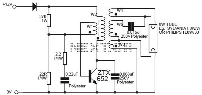
This circuit is essentially an 8W inverter circuit designed to drive an 8W fluorescent lamp from a 12V power supply. It utilizes an inexpensive inverter based on a ZTX652 transistor. The inverter will operate efficiently to convert the DC...

Fluorescent tubes contain mercury, which poses health risks. Improper disposal of these tubes is harmful to both the environment and health; therefore, recycling is a beneficial option. The 555 timer IC is utilized to generate a square wave voltage...
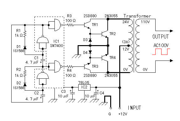
The circuit utilizes an integrated circuit (IC) type multivibrator as the oscillator for alternating current, operating at approximately 60 Hz. The 7400 IC is employed for this purpose, although the 7404 IC can also be used. The oscillator signal...
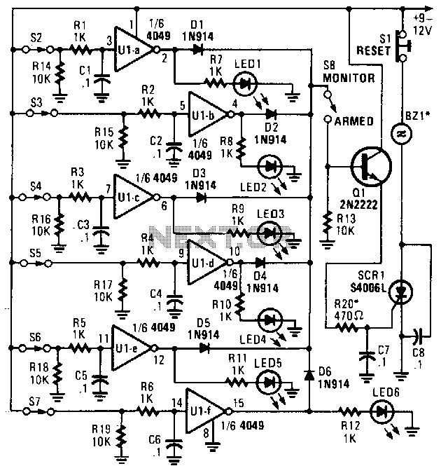
This alarm features status LEDs connected to each inverter output, which indicate the status of the corresponding sensor. S8 is utilized to monitor the switches through the LEDs or to activate an alarm using Q1 and SCR1. Additionally, BZ1...

The versatile circuit can be employed to achieve various functions, including an astable multivibrator, a monostable multivibrator, a switch debouncer, or a frequency discriminator. Inverters U1a and U1b are configured as a latch. When the input voltage (VIN) is...
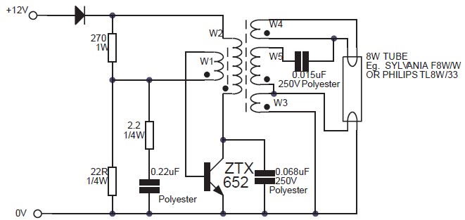
This circuit is an 8W inverter designed to drive an 8W fluorescent lamp from a 12V power supply, utilizing an inexpensive inverter based on a ZTX652 transistor. The inverter operates from power supplies ranging from 10V to 16.5V, achieving...