
PCB Parametric Audio Equalizer
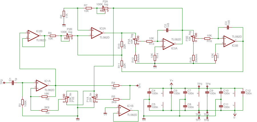
The parametric equalizer circuit is designed to provide precise control over audio frequencies, allowing for enhanced sound customization. The integration of the potentiometers directly onto the PCB minimizes signal degradation that can occur with long cable runs, thereby reducing noise and improving overall sound quality. Each potentiometer is strategically placed to ensure ease of access while maintaining a compact layout. The SMD technology utilized in this design not only streamlines the assembly process but also contributes to a smaller footprint, making it suitable for various applications where space is a constraint.
The circuit employs a series of operational amplifiers configured to create the desired filtering characteristics. The gain control adjusts the amplitude of the audio signal, while the frequency control allows users to select the center frequency of the filter. The width control, often referred to as Q, determines the bandwidth of the frequency being adjusted, enabling users to fine-tune the audio output to their preference. The stacked PCB design facilitates the implementation of multiple filtering stages, which can be tailored to target specific frequency ranges for more detailed sound shaping.
In summary, this compact, all-SMD parametric equalizer design significantly improves upon traditional designs by reducing complexity, enhancing sound quality, and providing users with precise control over their audio signals. The modifications made to the original design not only address practical assembly challenges but also optimize the performance and usability of the equalizer.This project is based on the parametric equalizer proposed by Elektor in the late 80s or early 90s and later published in the book "Creations electroniques" in 1993 (Publisher: Publitronic). Their design involved three stereo potentiometers per channel, which means a lot of cables from the front panel to the circuit board.
It`s quite tiedous to build and IMHO prone to noise from within the enclosure. To solve these problems and make the unit more compact I have put everything on a single board, potentiometers included. No more cables! A graphic equaliser has only one control per band: the gain. A parametric equaliser has 3 controls: gain, frequency and width. While a graphic equalizer requires a lot of bands to correct the sound, a parametric equaliser is more acurate and usually only one to three filters are used in series.
Several modifications were made to allow these improvements. First, it`s an all-SMD board: easier and cheaper to build. This is necessary because clearance is limited with the front pannel. More importantly, it is important to realize that several PCBs will be stacked next to each other for the different filtering stages (usually 3, as Elektor says) and therefor we have no space to extend the PCB without spacing the potentiometers too. The only other option would be to use DIL circuits and several stacked PCBs: not very practical or cost effective.
🔗 External reference
Related Circuits

In essence, it uses the same principle as a graphic equaliser, but the simulated inductors are made variable, so the frequency can be swept back and forth. The four 10K pots provide cut (when on the left or anti-clockwise...

Using the STK4038X audio amplifier IC, can be designed a very simple high power and efficiency audio power amplifier. This circuit is manufactured by Sanyo Corporation and will provide an output power of 60 watts on an 8 ohms...

Audio can be extracted from a telephone line using a transformer and a capacitor to isolate the line from external equipment. A non-polarized capacitor is placed in series with the transformer line connection to prevent direct current from flowing...
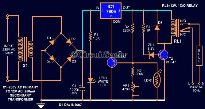
This circuit automates the control of street or porch lights. The automatic lamp controller circuit utilizes a 7806 voltage regulator IC, which can be employed to automate street lights, tube lights, or any other home electrical lighting systems. The...
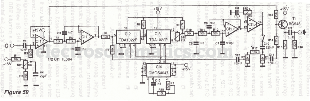
The first reverberator presented is based on the TDA1022, which is the most commonly used BBD (Bucket Brigade Device). Adjustments for proper functionality of the reverberator are required before connecting the power supply. The TDA1022 is a versatile BBD that...
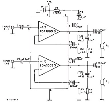
The TDA2005 car audio amplifier circuit is specifically designed for use in devices such as car radios and CD players. This amplifier circuit utilizes the TDA2005 audio integrated circuit (IC), which can deliver a maximum output power of 20...
Warning: include(partials/cookie-banner.php): Failed to open stream: Permission denied in /var/www/html/nextgr/view-circuit.php on line 713
Warning: include(): Failed opening 'partials/cookie-banner.php' for inclusion (include_path='.:/usr/share/php') in /var/www/html/nextgr/view-circuit.php on line 713