
Phone camera flash control circuit

The circuit operates on the principle of a capacitive charge pump, which is a type of DC-DC converter that steps up the input voltage to a higher output voltage using capacitors as energy storage elements. The AAT3110-4.5 chip is specifically designed for such applications, providing efficient voltage boosting while maintaining a compact design suitable for mobile devices.
In this application, the lithium battery, typically around 3.7V, is boosted to 4.5V, which is suitable for driving high-brightness LEDs. The output filter capacitor (4.7µF) smooths the output voltage, ensuring stable operation of the LEDs during the flash event. The storage capacitor (1µF) temporarily holds charge to provide the necessary current during the peak flash period.
Resistor R1 is crucial for balancing the current across multiple LEDs, ensuring uniform brightness and preventing any single LED from being overdriven, which could lead to premature failure. The peak current regulation resistor RP allows for fine-tuning of the flash intensity. By adjusting the resistance value of RP, the user can control the peak current flowing through the LEDs, thus adjusting the brightness of the flash according to specific requirements.
Overall, this circuit design is optimized for providing a reliable and adjustable flash for mobile phone cameras, enhancing low-light photography capabilities while ensuring efficient power management from the device's battery.200mA peak current letter phone photo camera flash circuit, using a AAT3110-4.5 electrical capacitive charge pump chip, the phone lithium battery voltage boost and regulated to 4.5V, to a group of light-emitting diode (LED) provide work for the voltage and 100 ~ 200mA peak current. The peak current through the switch as a flash of VF form a loop. The charge pump input filter capacitor capacitance of lOtiF, output filter capacitor electric capacity 4.
7vF, storage capacitor capacitance of ltiF. Ri, LED light-emitting tube balancing resistor. RP is the peak current regulation section resistance, adjust the resistance of RP can be set peak current size.
Related Circuits
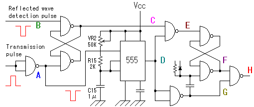
The alarm detector circuit operates differently from the Ultrasonic Alarm (1). In Ultrasonic Alarm (1), an alarm output is triggered by the detection of a reflected wave from an object during the setup time. Conversely, in this circuit, an...
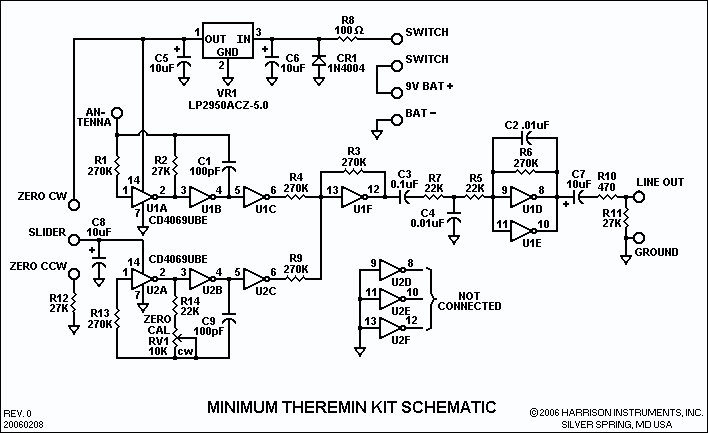
Two identical integrated circuits, U1 and U2, known as "hex inverters" are used for the theremin's primary functions. They are CMOS (Complimentary Symmetry Metal Oxide Semiconductor) devices, typically used in digital circuits to perform a logic function called "inversion."...
When the touch-on contacts are bridged, pin 6 of U1 goes low, which forces its output (the set output) at pin 4 to go high. That high divides along two paths; in one path, the output is applied to...

How to change the brightness of an LED. Are LED lights dimmable? Is it possible to adjust the brightness of LEDs? An LED is essentially a diode; when the forward voltage exceeds 0.7 volts, it begins to emit light,...

The circuit for a SIM card reader is presented here. It utilizes a CMOS hex inverter along with other basic components. Not only does it function effectively, but it is also capable of communicating with a PC through a...
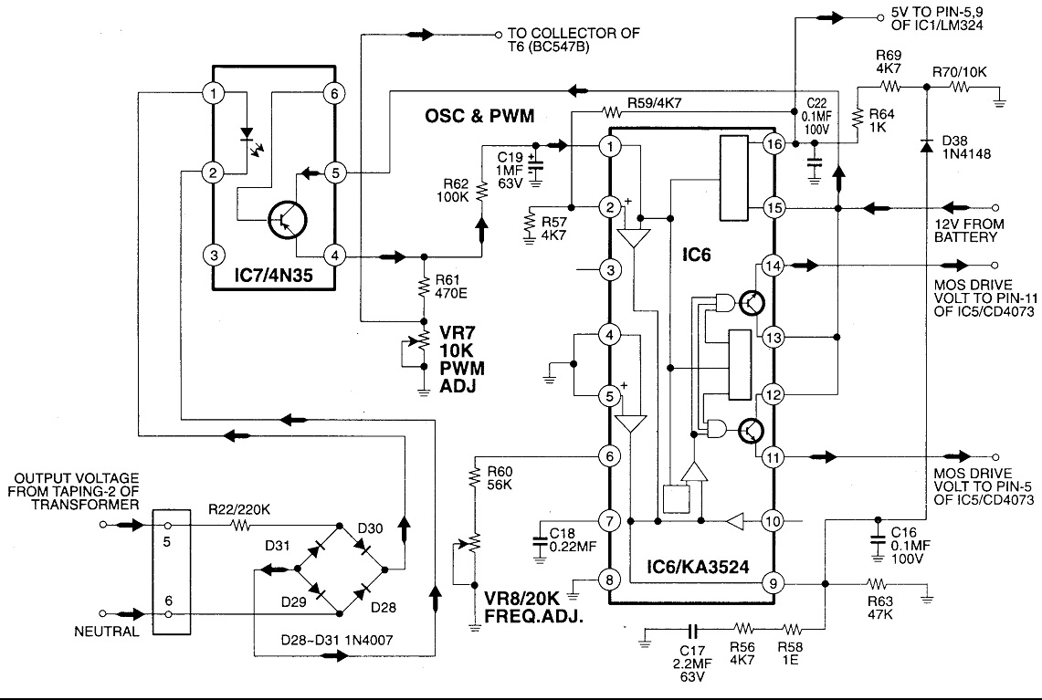
Circuit No. 1 (Oscillator Circuit and Feedback Circuit) Circuit No. 2 (MOS Driver Circuit) Final Product: - Operation of Circuit No. 1 (Oscillator Circuit and Feedback Circuit) This inverter utilizes Pulse Width Modulation (PWM) technology. The working principle of...