
Positive Voltage Doubler

The Positive Voltage Doubler circuit is designed to convert a lower input voltage into a higher output voltage, effectively doubling the input voltage. The MAX1044 and ICL7660 are integrated circuits that facilitate this process through charge-pump technology. The operation of the circuit involves the use of capacitors and diodes to store and transfer charge, resulting in an increased output voltage.
In this configuration, the circuit typically consists of two capacitors, C1 and C2, and a Schottky diode, D1. The input voltage is applied to the circuit, and during the first phase of operation, capacitor C1 charges to the input voltage level. In the next phase, the switch within the IC alternates, allowing C1 to discharge into C2 while simultaneously charging from the input voltage again. The Schottky diode is crucial in this process as it allows current to flow in one direction with minimal voltage drop, thus improving efficiency.
The output voltage across C2 will be approximately double the input voltage, minus the forward voltage drop of the diode. This circuit is particularly useful in applications requiring higher voltages from a standard lower voltage source, such as powering operational amplifiers or other analog components that require a higher supply voltage. The choice of components, particularly the Schottky diode, is essential for optimizing performance and minimizing losses in the circuit.
Overall, the Positive Voltage Doubler circuit using the MAX1044 or ICL7660 is an effective solution for applications needing increased voltage levels while maintaining compactness and efficiency.This is a simple circuit of Positive Voltage Doubler. This circuit uses the MAX1044/ICL7660. The schottky diode was chosen to reduces the voltage drop. This.. 🔗 External reference
Related Circuits
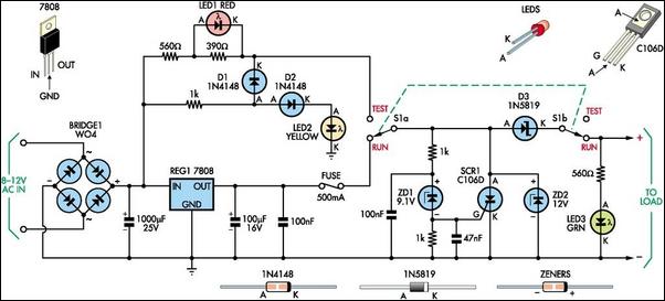
This 8V DC power supply is designed for use with high-end electronic equipment. It includes full over-voltage protection to safeguard against regulator failure, whether in the supply itself or in the connected device. The circuit employs a standard full-wave...
The Zener diode ZD1 monitors the supply voltage, and if the supply exceeds 6 V, transistor Q1 will activate. This activation causes transistor Q2 to conduct, thereby clamping the voltage rail. The subsequent behavior of the circuit is contingent...

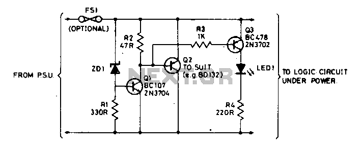
Applying voltage to the circuit triggers SCR1. With SCR1 on, the voltage on the anode of SCR2 rises until SCR2 triggers to commutate SCR1. The voltage on the gate of SCR1 will swing negative at this time, and only...
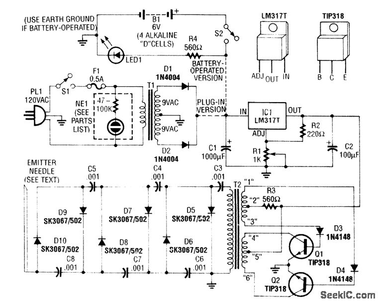
A modified black and white television flyback transformer is utilized in this circuit alongside a voltage multiplier to generate a negative voltage ranging from 9 kV to 14 kV. This high voltage is connected to a discharge needle to...
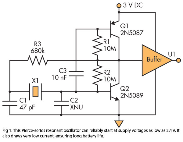
A Pierce (crystal) oscillator designed to deliver a stable clock signal for a minimum duration of one year when powered by battery voltages as low as 2.4 V. The Pierce oscillator circuit is a type of crystal oscillator that utilizes...
The battery voltage is 1V for a low-frequency amplifying circuit, which can operate with a power supply voltage ranging from 1V to 1.7V, making it suitable for use with small batteries. The circuit provides an output power of 80mW...