
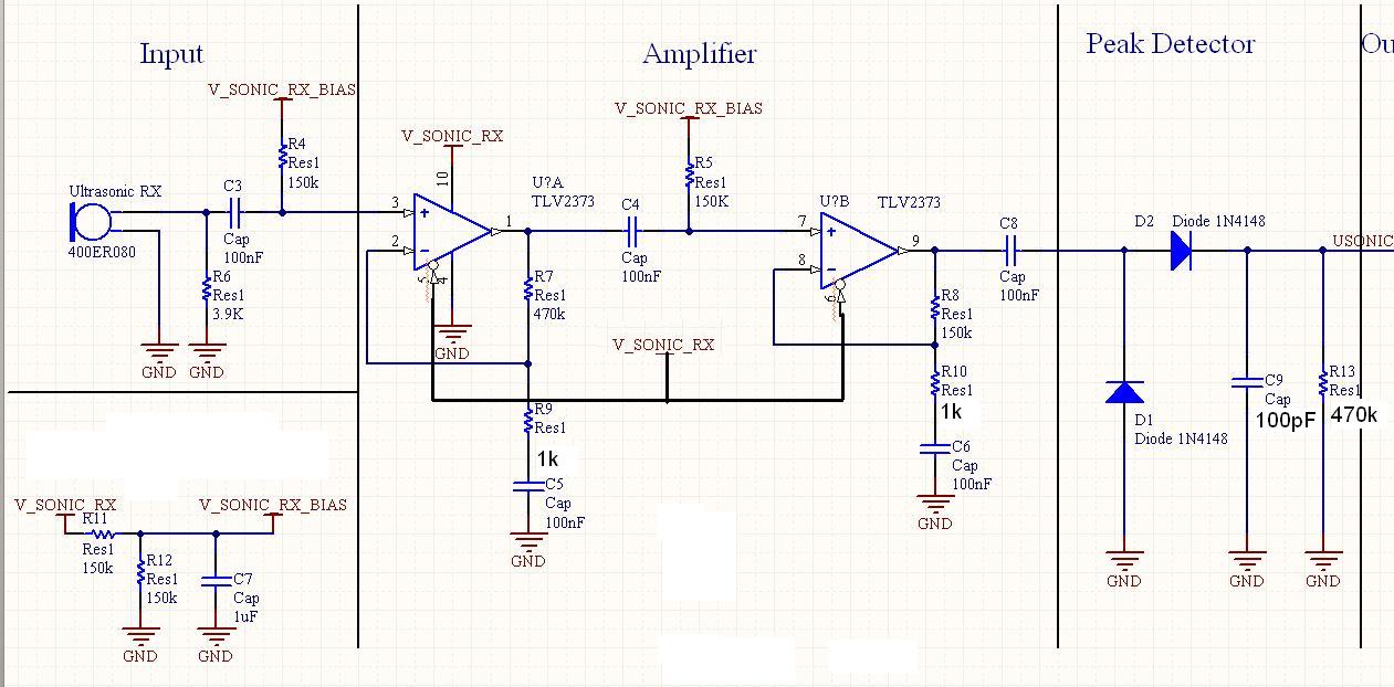
Precision Squarer

The squarer circuit is designed to convert an input signal into a square wave with a sharp transition between high and low states. It typically consists of components such as operational amplifiers, resistors, and capacitors, which work together to enhance the signal's characteristics.
The operational amplifier is often configured in a comparator mode, where it compares the input signal to a reference voltage. When the input signal exceeds the reference voltage, the output switches to the high state; conversely, when the input signal falls below the reference voltage, the output switches to the low state. This rapid transition results in a square wave output.
To ensure the squarer circuit provides a fast rise time, careful selection of components is essential. The feedback network, composed of resistors and capacitors, must be tailored to minimize propagation delay and optimize the circuit's frequency response. Additionally, the use of Schmitt trigger configurations can further enhance the circuit's performance by providing hysteresis, which prevents noise from causing unwanted oscillations in the output.
Applications of squarer circuits are prevalent in digital electronics, where clean square waves are essential for clock signals, pulse generation, and signal conditioning. The ability to produce a precise square wave from a noisy or distorted input signal makes this circuit invaluable in various electronic systems.Squarer circuit is used to shape signal, to get more defined square wave. This circuit is useful to make convert the signal so it has very fast rise time. Here.. 🔗 External reference
Related Circuits

The circuit employs negative feedback exclusively for positive signals. The inverting input receives feedback only when diode D1 is forward biased, which occurs solely with positive input signals. As the positive input signal increases, the output of the operational...
It has been mentioned that the operational amplifier (op amp) in the second stage may be damaged. Confirmation is requested by testing the op amp in a buffer configuration or any simple configuration. This test is necessary to ascertain...
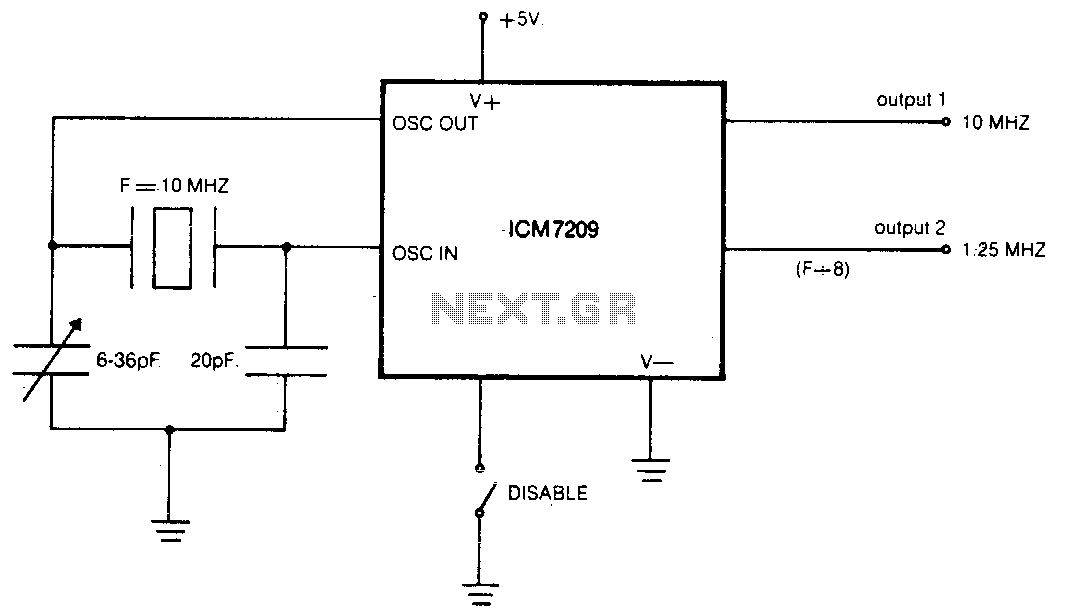
The CMOS IC directly drives five TTL loads from either of two buffered outputs. The device operates at up to 10 MHz and is compatible with bipolar, MOS, and CMOS technologies. The CMOS integrated circuit (IC) is designed to interface...
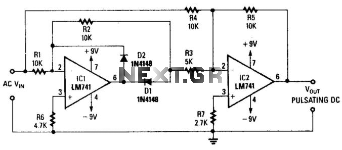
This circuit utilizes two operational amplifiers (op amps) to generate a full-wave rectified version of the input signal. Op amp IC1 inverts the negative-going signal, but due to diode D2, it remains close to zero. IC2 generates a positive-going...
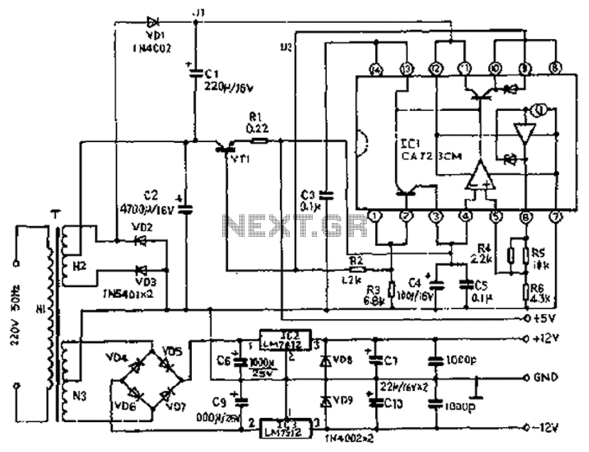
The circuit depicted features a secondary N3 center tap transformer (T) with a common point connecting diodes VD2 and VD3 to positive electrodes, along with capacitors C2, C6, C7, and negative electrodes connected to capacitors C9 and C10. Additional...

The loop gain of the operational amplifier (OP) is primarily influenced by the ratio of the input resistor to the feedback resistor. Consequently, any resistance error can lead to a corresponding gain error, which necessitates the use of high-precision...