
Protected Intrinsically Safe Op Amp Circuit

The advantage of this circuit is that, although it is designed as a unity gain buffer, the same techniques can be applied to inverting, non-inverting, or differential gain stages.
This circuit serves as a protective driving mechanism for external loads, ensuring safe operation under fault conditions. The operational amplifier (op-amp) is configured as a unity gain buffer, providing high input impedance and low output impedance, which is ideal for isolating the load from the driving circuitry. The two zener diodes are strategically placed to clamp any excessive voltage that may arise from the load, thereby protecting downstream components. The clamping voltage is set at 10 V, ensuring that the op-amp and other sensitive components are shielded from potentially damaging voltages.
Resistors R1, R2, and R3 play a crucial role in limiting the current flowing through the zener diodes and the op-amp. This current limiting is essential to prevent thermal runaway and damage to the components during fault conditions. The selection of resistor values should be based on the maximum expected load current and the zener diode specifications to ensure that all components operate within their safe limits.
Diode D1 is included to provide additional protection to the op-amp output stage. In the event that the clamp diodes are activated due to an overvoltage condition, D1 prevents reverse voltage from affecting the op-amp, thereby maintaining the integrity of the signal and the operational capability of the circuit.
The versatility of this circuit design allows it to be adapted for various configurations, including inverting, non-inverting, and differential gain stages, making it a robust solution for different applications requiring voltage clamping and current limiting features. This adaptability enhances its utility in a wide range of electronic systems where load conditions may fluctuate or where fault tolerance is necessary. The circuit is designed to drive an external load. A fault condition in the external load circuit could feed excessive current or voltage back into the line drive circuit. If excessive voltage appears from the load, the two zener diodes will clamp that voltage to a safe level, which in this case is 10 V.The current in the zener diodes, op amp, and the remainder of the circuitry is limited to a safe level by resistors Rl, R2, and R3.
D1 protects the op-amp output stage from 10 V appearing across the clamp diodes under a fault condition. The advantage of this circuit is that, although it`s designed as unity gain buffer, the same techniques can be applied to inverting, noninverting, or differential gain stages.
Related Circuits
A passive light-emitting diode output level indication circuit. This circuit utilizes a light-emitting diode (LED) to provide a visual indication of the output level from a given source. The design is characterized by its passive nature, meaning it does not...
In electronics, an H-bridge circuit refers to a configuration consisting of four individual switching devices, such as transistors or MOSFETs, which can be controlled by external discrete signals from the respective stages of the control circuit. During operation, the...
I am looking to build a timer for a pump. I want the pump to run for 5 minutes, then stop. To create a timer circuit for a pump that operates for a duration of 5 minutes, a simple astable...
The construction LED circuit illustrated in the figure requires manual power. Once powered, the light will blink to alert individuals to pay attention to safety. The circuit is designed to enhance safety awareness in construction environments by utilizing a blinking...
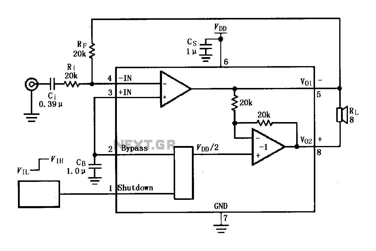
The LM4819 audio power amplifier is designed to amplify audio signals. An audio signal is input through the coupling capacitor (Ci) and the resistor (Ri) applied to the inverting input terminal (pin 3) of the amplifier. The inverting input...
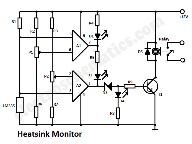
This heatsink temperature monitor circuit uses three LEDs to signal when the temperature exceeds two boundary levels. When the heatsink temperature is below 50-60°C (122-140°F), the green LED lights up. The yellow LED indicates that the temperature is between...