
Resistance-to-voltage converter

The described circuit is designed for high-impedance measurement applications, specifically targeting a maximum resistance of 20 megohms. The choice of a buffer amplifier with a low input bias current is crucial to minimize measurement errors caused by loading effects. The specified input bias current of less than 30 nA ensures that the amplifier does not significantly affect the circuit being measured, allowing for accurate readings.
The Siliconix L144 micropower triple op amp is an integral component of this design. By employing two of the three available amplifiers, the circuit can achieve both amplification and buffering functions. The first amplifier can be configured as a non-inverting amplifier to provide gain, while the second amplifier serves as a buffer to isolate the measurement circuit from the load. This configuration enhances the overall stability and accuracy of the measurement.
In practical applications, the circuit may be used in various settings, including laboratory measurements, sensor interfacing, and high-impedance data acquisition systems. The low power consumption of the L144 op amp makes it suitable for battery-operated devices, ensuring that the circuit remains efficient while delivering precise measurements. The careful selection of components and configuration allows for reliable performance in demanding electronic measurement tasks.Circuit will measure accurately to 20M when associated with a buffer amplifier (Al) having a low input bias current (IiN) < 30 nA) The circuit uses two of the three amplifiers contained in the Siliconix L144 micropower triple op amp.
Related Circuits
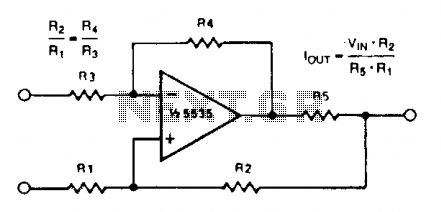
A simple voltage-to-current converter is illustrated. The output current is given by 0t or Vjn/R. For negative currents, a PNP transistor can be employed, and for improved accuracy, a Darlington pair can replace the transistor. With meticulous design, this...
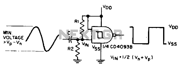
The sine input is AC coupled by capacitor C. Resistors Rl and R2 bias the input midway between Vn and Vp, which are the input threshold voltages. This configuration is designed to provide a square wave at the output. The...
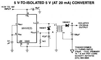
A negative output voltage DC to DC converter generates a -5V output at pin A. To achieve -5V at point A, the primary of the transformer must fly back to a diode drop more negative than -5V. If the...
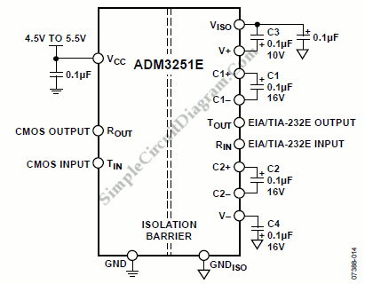
The ADM3251E is a transceiver that features high-speed operation, 2.5 kV full isolation, and a single channel for RS-232/V.28 communication. This device operates from a single 5 V power supply. The ADM3251E transceiver is designed for robust communication in environments...
This document outlines the layout considerations for switch-mode DC-DC converter printed circuit boards (PCBs) aimed at minimizing switching noise and electromagnetic interference (EMI). The layout of switch-mode DC-DC converter PCBs is critical in ensuring efficient operation and compliance with electromagnetic...
A substation capable of consuming 100 MVA with 375 kVA, 60 Hz input and 132 kV at 50 Hz using the same power. The challenge is to convert the 60 Hz input to 50 Hz, including a wiring diagram. To...