
5W PLL FM Transmitter (PIC16F627A)
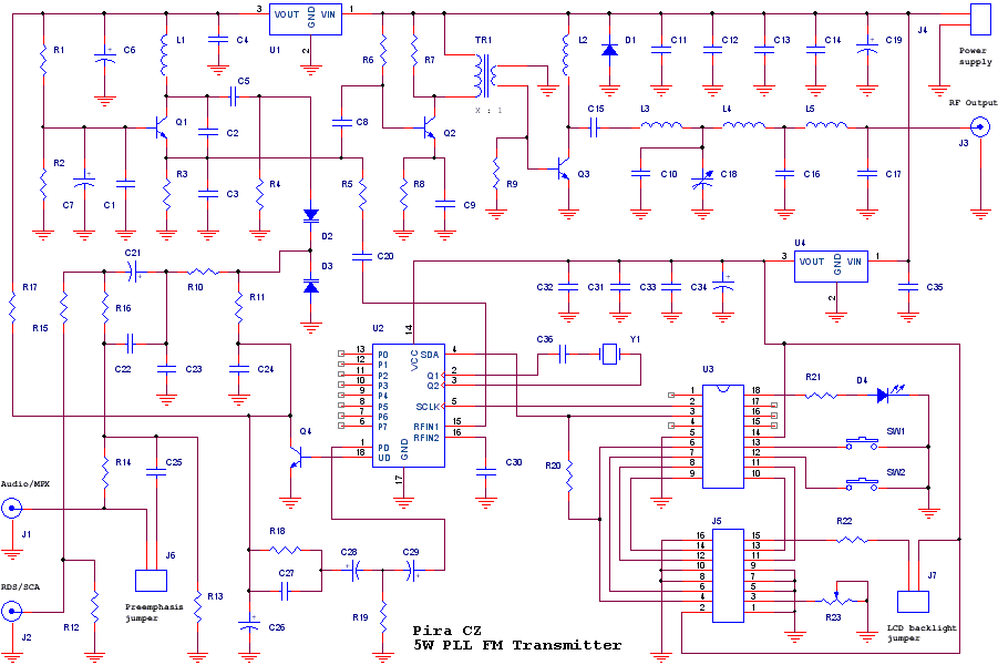
Wind all coils (except the L2) by a 0.8 mm wire.
The Y1 package must be tied to ground!
Make sure the Q3 terminals are as short as possible (about 2-3 mm above board). The 2N3553 case/heatsink can't be tied to ground!
Be careful when soldering smd capacitors!
To make the TR1 transformer, use specified number of turns on primary side and one turn on secondary side. The secondary wire should be quite thick but the primary can be as thin as you want. Wind on a 2-hole ferrite (material 61 or N1).
Q1 - BF240
Q2 - BFG135 (BFG235)
Q3 - 2SC1971 (2N3553) + heatsink
Q4 - BC547B
D1 - SB260 (1N5822, 1N581x)
D2, D3 - BBY40 (BBY31)
D4 - LED 5mm
U1 - 78L09
U2 - TSA5511 (TSA5512, SDA3202) in DIL socket
U3 - PIC16F627A in DIL socket (programmed)
U4 - 78L05
R1, R2, R11, R17, R20 - 10k
R3, R21 - 270R
R4, R10 - 4k7
R5, R7, R12, R13, R16 - 680R
R6, R14 - 18k
R8 - 47R (33R if Q2 is BFG235)
R9 - 18R
R15 - 33k
R18 - 3k3
R19 - 100k smd 1206
R22 - 91R
R23 - trimmer 5k mini
C1, C4, C9, C12, C13, C14, C15, C30, C31, C32, C33, C35 - 10n smd 1206 (C)
C2, C20 - 15p (C)
C3 - 10p (C) (15p if the PCB is single-sided)
C5, C22 - 330p (C)
C6, C28, C29, C34 - 100u/10V (E)
C7, C26 - 10u/35V (E)
C8, C17 - 22p (C)
C10, C16, C23, C24 - 47p (C)
C11, C27 - 100n (C)
C18 - cap. trimmer 50p
C19 - 470u/16V (E)
C21 - 4u7/50V (E)
C25 - 3n3 (P)
C36 - 27p (C)
L1 - 3.5 turns on 7 mm diameter
L2 - 1uH/815mA choke, or about 10 turns of thin wire on mini ferrite core
L3 - 2.5 turns on 6 mm diameter (4.5 turns if Q3 is 2N3553)
L4, L5 - 3.5 turns on 6 mm diameter, coil length 5 mm
Y1 - crystal 6.4 MHz or 3.2 MHz
TR1 - rf ferrite transformer 2:1 (3:1 if Q3 is 2N3553), see text
SW1, SW2 - button mini
J1, J2, J3 - BNC connector 90 deg.
J4 - power supply connector
J5 - HD44780 LCD standard connector, 2x8 or 2x16 characters
J6, J7 - jumper
The described transmitter circuit is designed for FM broadcasting, incorporating features such as RDS/SCA input and Audio/MPX input with an optional preemphasis stage. The flexibility of operation with or without a stereo encoder allows for versatile applications. Tuning is facilitated by dual-speed PLL controlled through two buttons, providing a user-friendly interface for adjusting frequencies across the FM band.
The circuit can function without an LCD display, making it suitable for various setups. However, it is advised that users possess prior experience in assembling similar electronic devices to ensure correct assembly and functionality. Upon completion of component placement, thorough checks for shorts between tracks and correct orientation of polarized components, particularly electrolytic capacitors, are crucial.
The tuning mechanism requires a crystal oscillator, with options for either a 3.2 MHz crystal for finer tuning steps of 0.05 MHz or a 6.4 MHz crystal for larger 0.1 MHz steps. The use of other crystal frequencies is not permissible, emphasizing the importance of adhering to specified components.
Coil winding is specified with a 0.8 mm wire, and careful attention is required when soldering surface-mount capacitors to avoid damage. The RF transformer (TR1) is constructed with a defined number of turns on the primary and a single turn on the secondary, utilizing a ferrite core of specified material for optimal performance.
The circuit employs various semiconductor components, including transistors (BF240, BFG135, 2SC1971, BC547B) and diodes (SB260, BBY40), which are critical for signal processing and amplification. Voltage regulators (78L09, 78L05) are included to provide stable power supply levels, while a programmed PIC16F627A microcontroller manages the overall operation.
Resistors and capacitors throughout the circuit are chosen for their specific values to ensure proper functioning of the transmitter, with careful attention to their placement and orientation. The design also includes specific inductors, with defined turns and diameters, to achieve the desired inductance values for RF applications.
Connectors for power supply and antenna are standard, ensuring compatibility with common equipment. The inclusion of jumpers allows for circuit modifications or configurations as needed, enhancing the versatility of the design. Overall, the circuit is a comprehensive solution for FM transmission, requiring careful assembly and adherence to specifications for optimal performance.The transmitter includes RDS/SCA input and Audio/MPX input with optional preemphasis. It can be used with or without stereo encoder. Tuning over the FM band is provided by two buttons that control dual-speed PLL. The transmitter can work also without the LCD display. Some experience with building devices of this kind are highly recommended. After complete parts placement: Check that there are no shorts bridging adjacent tracks or pads. Check electrolytic capacitors polarity and semiconductor parts orientation. Make any duty load and connect it temporarily to the antenna connector. Use for example 2 or 3 bulbs (24V/170mA or 24V/3W) in parallel. For 0.05 MHz tuning step a 3.2 MHz crystal is required. In other case a 6.4 MHz crystal will make good work (tuning step 0.1 MHz). Any other crystal cannot be used. Wind all coils (except the L2) by a 0.8 mm wire. The Y1 package must be tied to ground! Make sure the Q3 terminals are as short as possible (about 2-3 mm above board). The 2N3553 case/heatsink can't be tied to ground! Be careful when soldering smd capacitors! To make the TR1 transformer, use specified number of turns on primary side and one turn on secondary side. The secondary wire should be quite thick but the primary can be as thin as you want. Wind on a 2-hole ferrite (material 61 or N1). Q1 - BF240 Q2 - BFG135 (BFG235) Q3 - 2SC1971 (2N3553) + heatsink Q4 - BC547B D1 - SB260 (1N5822, 1N581x) D2, D3 - BBY40 (BBY31) D4 - LED 5mm U1 - 78L09 U2 - TSA5511 (TSA5512, SDA3202) in DIL socket U3 - PIC16F627A in DIL socket (programmed) U4 - 78L05 R1, R2, R11, R17, R20 - 10k R3, R21 - 270R R4, R10 - 4k7 R5, R7, R12, R13, R16 - 680R R6, R14 - 18k R8 - 47R (33R if Q2 is BFG235) R9 - 18R R15 - 33k R18 - 3k3 R19 - 100k smd 1206 R22 - 91R R23 - trimmer 5k mini C1, C4, C9, C12, C13, C14, C15, C30, C31, C32, C33, C35 - 10n smd 1206 (C) C2, C20 - 15p (C) C3 - 10p (C) (15p if the PCB is single-sided) C5, C22 - 330p (C) C6, C28, C29, C34 - 100u/10V (E) C7, C26 - 10u/35V (E) C8, C17 - 22p (C) C10, C16, C23, C24 - 47p (C) C11, C27 - 100n (C) C18 - cap.
trimmer 50p C19 - 470u/16V (E) C21 - 4u7/50V (E) C25 - 3n3 (P) C36 - 27p (C) L1 - 3.5 turns on 7 mm diameter L2 - 1uH/815mA choke, or about 10 turns of thin wire on mini ferrite core L3 - 2.5 turns on 6 mm diameter (4.5 turns if Q3 is 2N3553) L4, L5 - 3.5 turns on 6 mm diameter, coil lenght 5 mm Y1 - crystal 6.4 MHz or 3.2 MHz TR1 - rf ferrite transformer 2:1 (3:1 if Q3 is 2N3553), see text SW1, SW2 - button mini J1, J2, J3 - BNC connector 90 deg. J4 - power supply connector J5 - HD44780 LCD standard connector, 2x8 or 2x16 characters J6, J7 - jumper
🔗 External reference
Related Circuits
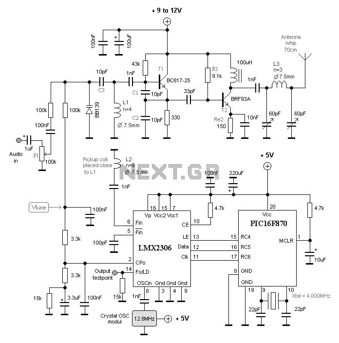
This transmitter is PLL controlled and the frequency is very stable and can be programmed digitally. The transmitter will work from 88 to 108 MHz and the output power is up to 500mW. With minor changes the frequency can...
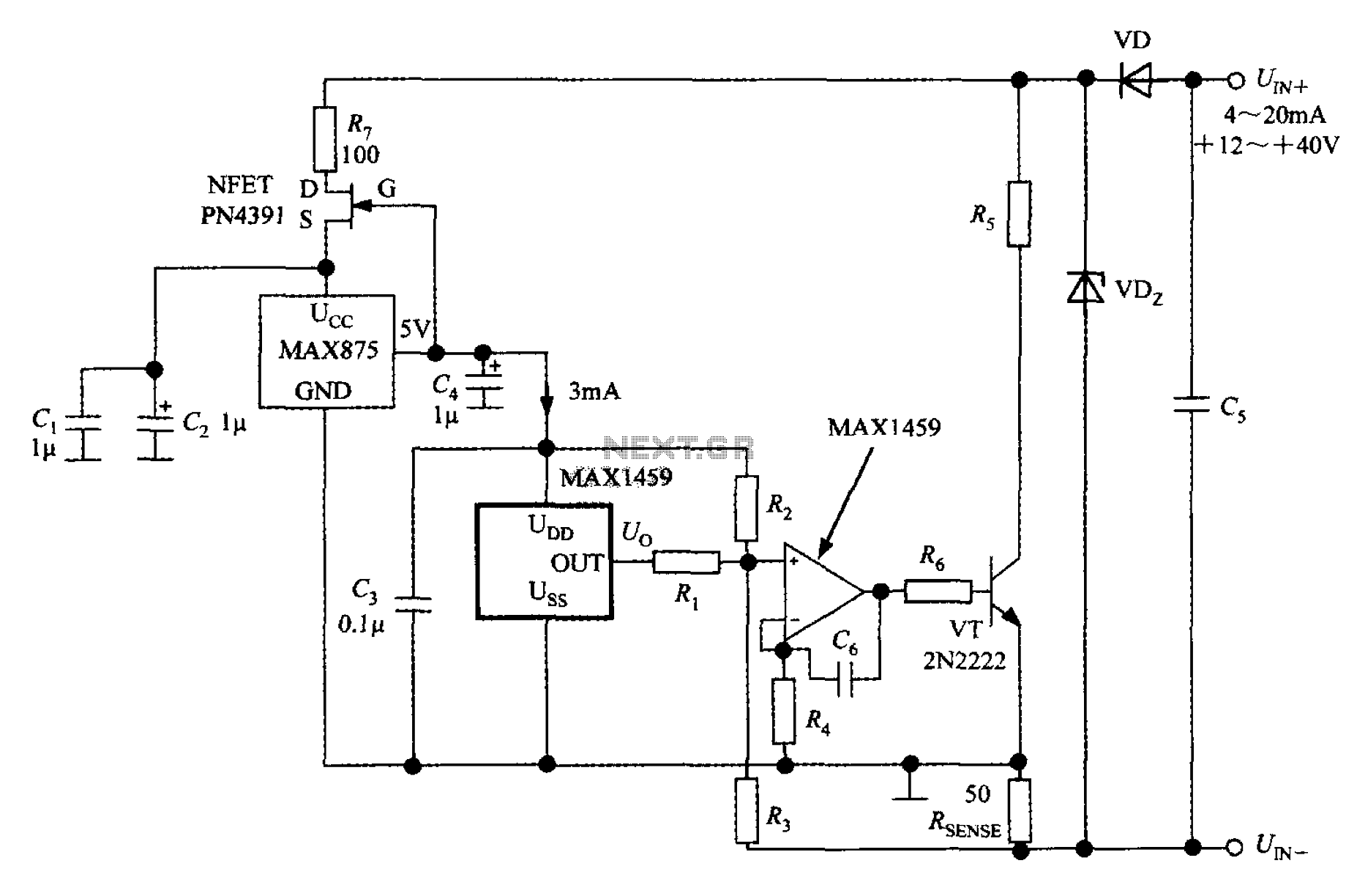
A 4 to 20 mA current transmitter circuit is implemented using the MAX1459, as illustrated in the accompanying figure. The output voltage from the programmable gain amplifier (PGA) is supplied to a spare amplifier chip, and subsequently, an external...

The circuit diagram of a simple FM transmitter utilizing a transistor is presented. While this design may not guarantee exceptional performance or range, it serves as a fundamental example. The circuit employs a general-purpose radio frequency transistor, the BF...

This infrared transmitter utilizes pulse width modulation (PWM). The transmitter is equipped with an LM567 tone decoder circuit. An audio signal (at least 50 mV peak-to-peak) is amplified with transistor T1 and subsequently used to modulate IC1. The frequency...
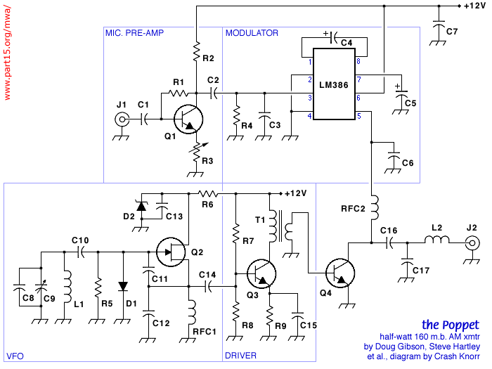
The Poppet is a half-watt AM transmitter designed by Mr. Doug Gibson of England. The original design was published in issue 84 of SPRAT, the newsletter of the GQRP Club. The version presented here incorporates modifications suggested by Steve...
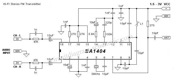
The following circuit illustrates the IC BA1404 used in a stereo FM transmitter circuit diagram. Features include ease of construction, making it accessible for anyone to build. The BA1404 is a versatile integrated circuit designed specifically for FM transmission applications....