
Schematic Diagram LM4992 bassed Stereo audio power amplifier circuit and explanation

The LM4992 is a highly efficient stereo audio power amplifier specifically designed for portable applications. It operates on a low voltage supply of 5V DC, making it suitable for battery-powered devices. The amplifier can deliver up to 1 watt of power per channel into an 8-ohm load, ensuring adequate sound output for small speakers or headphones.
One of the notable advantages of the LM4992 is the elimination of output coupling and bootstrap capacitors, which simplifies the circuit design and reduces the overall component count. This feature not only saves space on the PCB but also minimizes power loss and improves efficiency, which is critical for portable devices that rely on battery power.
The amplifier includes independent shutdown controls for each channel, allowing for enhanced power management. When a channel is not in use, it can be disabled, significantly reducing power consumption. This feature is particularly beneficial in applications where battery life is a concern.
Thermal management is another critical aspect of the LM4992 design. The internal thermal shutdown protection mechanism prevents the amplifier from overheating, thereby safeguarding both the device and the user. This feature is essential for maintaining reliability and performance during prolonged use.
Additionally, the advanced pop & click circuitry integrated into the LM4992 minimizes audible noise during power-up and power-down sequences, enhancing the user experience. The amplifier is also unity-gain stable, meaning it can be configured to operate at a gain of 1 without oscillation, which simplifies the design process for various applications.
For applications requiring specific gain settings, external resistors can be utilized to configure the amplifier's gain, providing flexibility in design. This adaptability, combined with the low power consumption and robust features, makes the LM4992 an excellent choice for developers designing portable electronic audio solutions.Using the LM4992 stereo audio power amplifier you can design a very simple audio power amplifier electronic project, that can be used for portable electronic devices. This power audio amplifier circuit is capable of delivering 1 watt, per channel, of continuous average power to an 8ohms BTL load with less than 1% distortion (THD+N) from a 5VDC
power supply. The LM4992 does not require output coupling capacitors or bootstrap capacitors, and therefore is ideally suited for mobile phone and other low voltage applications where minimal power consumption is a primary requirement. Some of the main features of the LM4992 audio amplifier designed for portable electronic devices are : independent shutdown control for each channel and a low-power consumption shutdown mode, internal thermal shutdown protection mechanism, advanced pop & click circuitry, unity-gain stable and can be configured by external gain-setting resistors.
🔗 External reference
Related Circuits
Frequency converter schematic, frequency to voltage converter schematic, frequency to voltage converter using TR, voltage to frequency converter application. A frequency converter is an essential electronic circuit that transforms frequency signals into corresponding voltage levels or vice versa. The frequency...
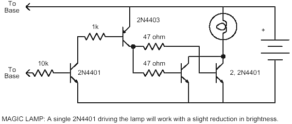
This magic lamp appears to be an ordinary frosted light bulb with a rather unusual characteristic. Whenever a finger touches the base threads and center contact, the lamp magically lights up without wires. It creates a compelling illusion if...
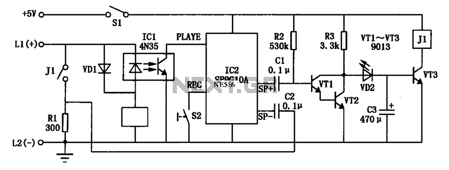
An automatic telephone responder circuit is illustrated. It incorporates a 10-second voice recording circuit (SR9G10A) activated by the power switch (S2). The circuit utilizes an electret microphone (IC2) for sound input. To initiate the response, the user must press...

The circuit consists of a few components, specifically four, to create a miniature wireless FM microphone. It operates with a stable frequency, achieving a range of over 10 meters with a 1.5V supply and a current consumption of less...
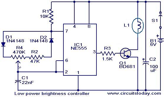
The circuit presented here is designed to control the brightness of low-power incandescent lamps. It utilizes the NE555 integrated circuit, configured as an astable multivibrator with a variable duty cycle. The output from the IC is connected to the...
This circuit is designed to connect stereo outputs from four different sources or channels as inputs, allowing only one of them to be selected and connected to the output at any given time. When the power supply is turned...