
Sine-Wave Vco Circuit

The circuit operates by utilizing a DC control voltage to modulate the resistance within the feedback network, which is comprised of capacitors C4, C3, C1 and resistors R12, R3. This modulation affects the overall gain and stability of the feedback loop, allowing for dynamic adjustment of the circuit's performance characteristics.
The capacitors, C4, C3, and C1, play a crucial role in determining the frequency response of the circuit, while resistors R12 and R3 are integral in setting the biasing conditions for the transistors Q2 and Q3. These transistors function as the oscillator elements, generating a periodic waveform that can be used for various applications, such as signal modulation or clock generation.
The feedback network's design is essential for ensuring that the oscillators remain stable and operate within the desired frequency range. By varying the DC control voltage, the effective resistance can be altered, which in turn influences the oscillation frequency and amplitude. This approach allows for fine-tuning of the circuit's output, making it adaptable to different operational requirements.
Overall, the described circuit demonstrates the interplay between control voltages and feedback components, highlighting the importance of careful design in achieving reliable and efficient oscillator performance. A dc control voltage varies the effective resistance iri feedback network C4/C3/C1 and R12/R3. Q2/Q3 are the oscillator transistors.
Related Circuits

To avoid excess ripple output on a power supply feeding a heavy load, usually a large value capacitor is chosen following the rectifier. In this circuit, C1 is only a 470uF capacitor. The gyrator principle uses the effect that...
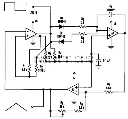
This function generator, based on an LT1016 high-speed comparator, will generate from a single +5-V supply. The slow rate of the op-amps used determines the maximum usable frequency of this circuit. The function generator utilizes the LT1016 high-speed comparator to...

Figure 1-30 illustrates an example of an output capacitor-less (OCL) power amplifier circuit, which can be analyzed as follows: In this circuit, transistors VTi and VTz form a single-ended input and a differential input single-ended output amplifier configuration. The...
A printed circuit board (PCB) was presented along with a schematic detailing the arrangement of components required for the activation of an LED on the board. The purpose of the PCB is to facilitate planning for the eventual construction...
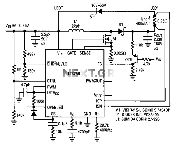
Common LED driver requirements include a wide and overlapping range of LED string voltages and input voltages. Many designers prefer to use an LED driver circuit that accommodates various battery power sources and multiple LED strings. This universal configuration...
I have been researching a "mystery circuit" and I cannot determine its name. Assistance is requested. The inquiry pertains to an unidentified electronic circuit, often referred to as a "mystery circuit." Such circuits can encompass a wide range of configurations...