
SmartCard adapter / interface for PC

The smartcard adapter is designed to comply with ISO 7816 standards, facilitating connections between computers and ISO 7816 compatible chip card systems, such as GSM mobile phones and pay-TV decoding systems, using the asynchronous half-duplex T=0 protocol. The adapter features a compact design to accommodate the physical dimensions of chip cards, which are standardized at 85.60 mm by 53.98 mm with a thickness of 0.76 mm and rounded edges. The adapter utilizes a MAX232 integrated circuit to convert RS-232 voltage levels to TTL levels, allowing for seamless communication between the smartcard and the computer. This conversion is essential for maintaining proper voltage levels during data transmission.
The adapter's circuitry includes essential components such as the 74LS07 open collector TTL driver, which ensures that the I/O line operates in a high impedance state when idle, preventing potential short circuits. Additionally, the design incorporates LEDs for visual feedback on the activation of the interface and data traffic, enhancing user interaction. The recommended PCB specifications emphasize the importance of adhering to precise dimensions to ensure compatibility with card slots, while also allowing for the integration of necessary electronic components.
The overall design prioritizes safety and reliability, advising users to check GND potentials before connecting devices and recommending the use of isolating RS-232 drivers for enhanced protection against voltage spikes. The careful arrangement of the adapter's components and the inclusion of protective features ensure a robust interface for smartcard communication.This smartcard adapter follow exactly the specification ISO 7816. Also, the protocol is the "asynchronous half duplex T=0 protocol" with "active low reset" and "inverse convention" as defined in this standard. The following description may be used in order to connect computers to ISO 7816 compatible chip card systems (e.g.
GSM mobile phones or other pay-TV decoding systems) if they also use asynchronous transmission. For smart card systems which use synchronous transmission (e.g. most phone cards) the interface described here will need some modifications. According to ISO, a chip card is 85.60 mm long, 53.98 mm high, 0.76 mm thick and the edges are rounded with a radius of 3.18 mm. It has eight defined contact areas (C1 - C8 in the diagram below), each of which is at least 2 mm wide and 1.7 mm heigh.
The pins DTR, DSR and CTS are not actually needed, they are just connected together in the adapter, so that defined levels are available on them because some software might need this. The MAX232 converts the RS-232 levels (about +10 and -10 V) to TTL voltage (0 and +5 V) and vice versa without requiring anything else than +5 V power supply.
This chip contains two TTL->RS-232 and two RS-232->TTL drivers and needs four external 1 uF capacitors in order to generate the RS-232 voltage internally. The adapter electronic gets its power supply from the smartcard reader device VCC line or you can use an external 5 V supply if you wish.
The card slot's RST line is connected using one of the TTL->RS-232 drivers in the MAX232 to DCD, so that the software and the reader can easily resynchronize in case of a protocol error. The I/O line is a bidirectional half-duplex asynchronous TTL level serial port. We can connect this line to a MAX232 TTL input driver (which is connected to RxD and sends bytes to the PC) in order to receive data from the reader.
The TxD signal is converted in the MAX232 to TTL level and is connected with an open collector TTL driver to I/O. This open collector driver (one of six in the 74LS07) has a high impedance output during idle state and 1 and is connected to GND during a 0 on it's input.
As there is already a pull-up resistor to +5 V on I/O in the smartcard reader device, this circuitry guarantees, that the adapter is in high impedance state if the TxD line is idle and delivers the correct voltage if the PC sends bytes and the smartcard reader device is in reception mode. As we don't connect totem-pole or tristate outputs to I/O, a short circuit should be impossible in the adapter.
Normally, both the RS-232 interface and the smartcard reader device slot should not be harmed by short circuits, but be careful. Also try to avoid electrostatic voltage (e.g. generated by walking on a suitable carpet) near the interface, because discharges cause easily reader or PC crashes and could theoretically even harm the hardware (especially CMOS chips like the 74HC04).
Before connecting the reader and the PC the first time, you might want to check the voltage between the two GND lines. In correct installations, the difference of the GND potentials is very low (below 1 V), but someone has reported up to 50 V (high impedance only).
Most smartcard reader devices are not connected with the earth line, so their GND potential is floating or sometimes only defined by e.g. the shielding of the antenna cable. If your antenna system is not correctly installed, the shield might also not be grounded. One quick solution might be to switch off all components and then connect first the RS-232 GND line to the GND of your smartcard reader device before connecting anything else.
BASE 0.5-0.8 mm PCB single sided U1 IC Maxim MAX232CPE (or Linear Technology LT1081CN) U2 IC 74LS07 (or 7407) C1,C2,C3,C4,C5 capacitors 1 uF (or higher), 16 V R1,R2 resistors 220 Ohm D1 diode LED standard RED D2 diode LED standard GREEN CON1 female Sub-D connector (9 or 25-pin) CAB4 pin + shield low voltage computer cable You might also design the ISO contacts on the PCB so that GND touches all pins at first when the PCB is inserted in the card slot. The only really secure protection between your PC and your smartcard reader device would be to use an isolating RS-232 driver (e.g.
you might want to check data sheets of Maxim's MAX250/251/252 chips which offer RS-232 protection up to 1500 V), but under normal circumstances you won't need this. Pay attention to the polarity of the capacitors (marked with a + in the diagram next to each capacitor)!
The -->-- symbols in the MAX232 diagram above indicate the voltage converters inside the chip. The RED LED show you when the reader activates the interface. The GREEN LED show you the I/O traffic. The capacitor between VCC and GND is not absolutely necessary but recommended. You can produce your card adapter by making a PCB with contact areas at the above listed locations. The PCB must have precisely the thickness and width of a real card, but it may be longer, so that you can locate the interface electronics on the part which remains outside the slot. Normal PCBs are about 1.3 mm think and won't fit into the slot. Either you get a PCB which is about 0.8 mm thick or you make it thinner, e.g. by using a sander machine. The adapter will only need the card contacts I/O, GND, RST and VCC. 🔗 External reference
Related Circuits
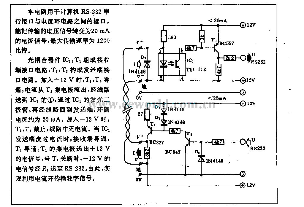
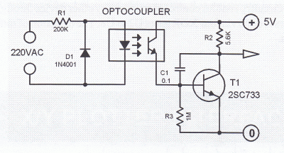
This circuit is utilized in RS-232 serial interface and current loop circuit applications. It converts voltage signals into a 20mA current signal, with a maximum transmission rate of 1200 bits per second. The CCD IC1 and transistor T1 form...
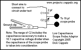
The capacitance between the wire and the probe would form a capacitive voltage divider with the probe's input capacitance, and at frequencies significantly higher than the low frequency roll off created by the probe's input capacitance and the probe's...
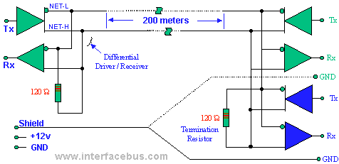
The CAN Bus interface utilizes an asynchronous transmission scheme that is regulated by start and stop bits at the beginning and end of each character. This interface operates using serial binary interchange, allowing information to be transmitted from transmitters...
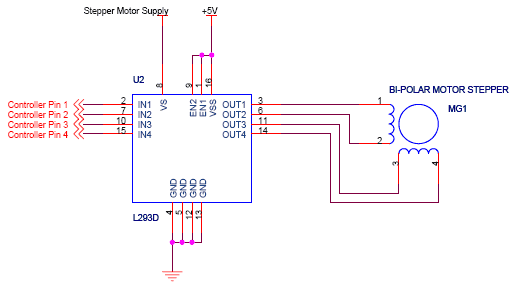
The circuit features four pins labeled "Controller pin 1," "Controller pin 2," "Controller pin 3," and "Controller pin 4," which are responsible for controlling the motion and direction of the stepper motor based on the step sequence programmed into...
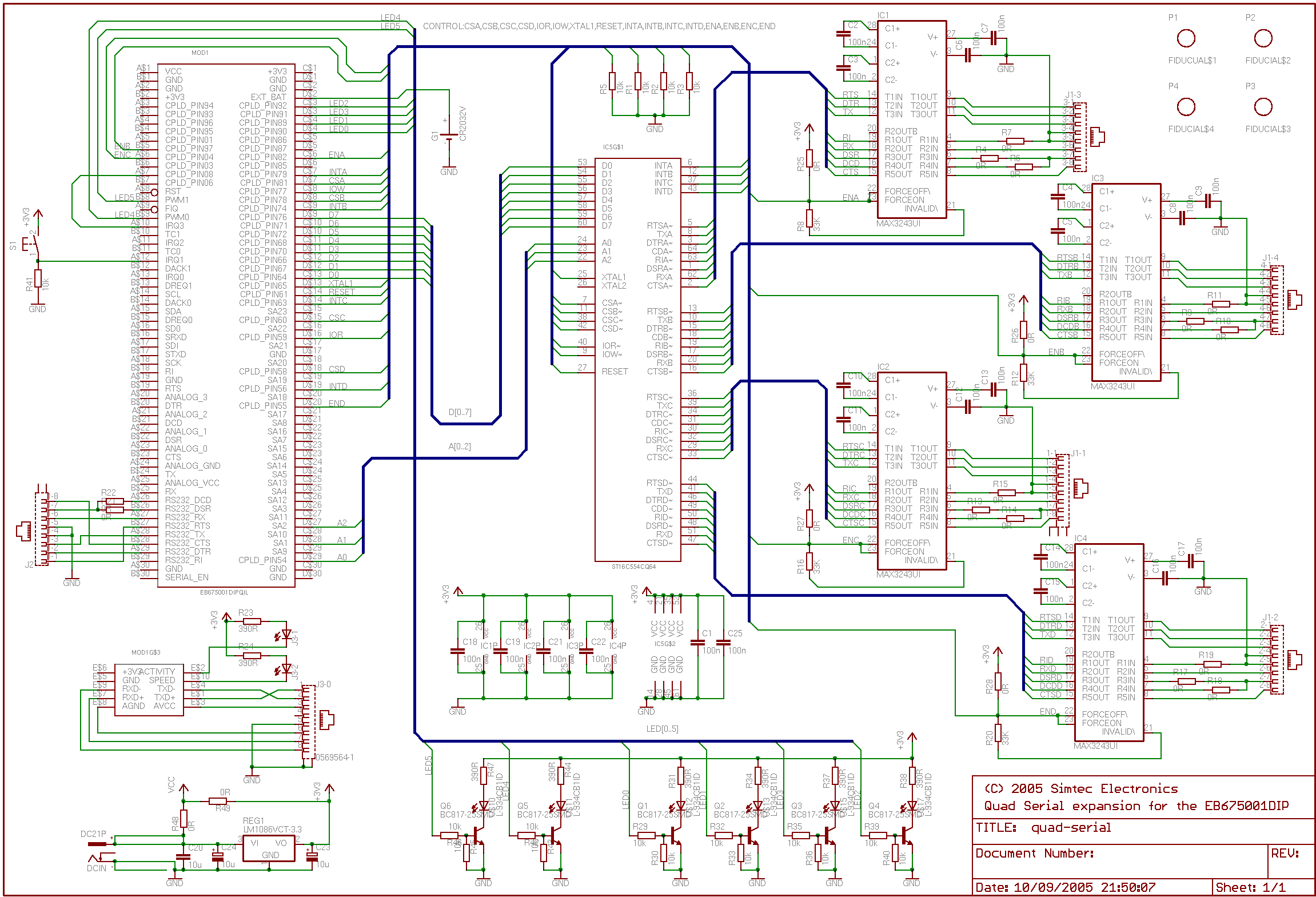
This application note details the integration of a quad serial controller into the EB675001 Module. A multi-source quad Universal Asynchronous Receiver and Transmitter (UART), specifically the 16554 type, was chosen to facilitate component sourcing and implementation. The RS232 line...
Many microcontroller designs typically integrate various interfacing methods. A microcontroller (µC) system can be viewed as a system that reads from inputs. Microcontroller systems are versatile platforms that facilitate the integration of multiple interfacing methods to interact with various peripherals...