
Squib-firing circuit 2

The described circuit utilizes an LRC input network to effectively manage the rate of voltage change (dv/dt) at the anode, ensuring it remains below the critical threshold of 30 V/μs. This is essential for protecting sensitive components from rapid voltage spikes. Resistor Rl is strategically placed to provide critical damping, which mitigates the risk of voltage overshoot that could lead to circuit instability or damage.
In scenarios where a simple RC filter might suffice, the high current demands of the squib necessitate the use of a low-resistance value combined with a larger capacitance. This configuration is designed to handle the substantial current without compromising performance. Resistor R3 plays a vital role in DC bias stabilization, maintaining steady operating conditions for the circuit. Capacitor C3 serves as a stiff gate bias source, ensuring that during the transient period when the anode voltage is applied, the gate of the SCR receives sufficient bias to trigger reliably.
The SCR is activated one second after the arming process through a straightforward R2C2Z1 time delay network, which provides a controlled delay before the SCR is fired, allowing for system readiness and safety checks. Additionally, resistor R4 is incorporated as a load for the SCR during testing phases when the squib is disconnected. This resistor limits the current flowing through the SCR, ensuring that it operates within its continuous rating, thus preventing potential damage during testing.
For operational flexibility, the circuit can be reset by interrupting the +28 V supply, followed by re-arming the system. This reset capability is crucial for maintaining the reliability and safety of the circuit, allowing for repeated testing and operational adjustments as necessary. Overall, this circuit design effectively balances performance, safety, and testing requirements.The LRC input network limits the anode dv/dt to a safe value—below 30 V/jus. Rl provides critical damping to prevent voltage overshoot. While a simple RC filter section could be used, the high current required by the squib would dictate a small value of resistance and a much larger capacitor. Resistor R3 provides dc bias stabilization, while C3 provides stiff gate bias during the transient interval when anode voltage is applied.
The SCR is fired one second after arming by means of the simple R2C2Z1 time delay network. R4 provides a load for the SCR for testing the circuit with the squib disconnected—limiting the current to a level well within the continuous rating of the SCR. The circuit can be reset by opening the +28 V supply and then re-arming.
Related Circuits
The following circuit illustrates a LEGO Light Sensor Circuit Diagram. This circuit is based on the LM358 integrated circuit, which features a dual operational amplifier and high-speed capabilities. The LEGO Light Sensor Circuit utilizes the LM358, a versatile dual op-amp...
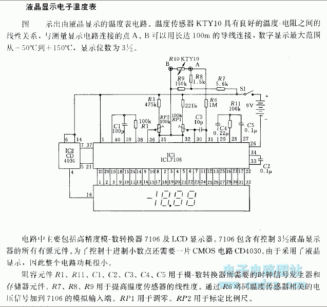
Related components PDF download: ICL7106CD4036. The LCD electronic thermometer circuit is illustrated. The temperature sensor KTY10 exhibits a strong linear relationship between temperature and resistance. Points A and B (Measurement display circuit) can be connected with a 100-meter wire....
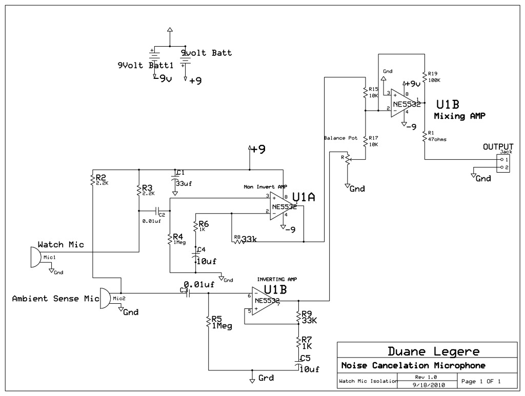
A microphone is designed to listen to a wristwatch while canceling ambient noise in the room. A circuit has been included, which is based on a headphone cancellation circuit. The schematic will be provided shortly. The suggested approach is...

The circuit consists of the MAX1494 digital strain gauge, as illustrated in Figure 5-31. It includes a bridge formed by resistance strain gauges and a temperature compensation sheet. The standard quasi-resistance values Rl and R are incorporated into the...

This gated 1-kHz oscillator provides press-to-turn-off functionality, along with waveforms available at the output of pin 3 and across capacitor C1. The gated 1-kHz oscillator circuit is designed to generate a square wave output at a frequency of 1 kHz....
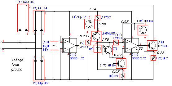
Application of the differential amplifier circuit in a simple small oscilloscope. The differential amplifier circuit is a crucial component in the design of a simple small oscilloscope. This circuit is designed to amplify the difference between two input voltage signals...