
TDA6103Q having a feedback factor of the test circuit

The TDA6103Q is a versatile integrated circuit primarily used in video signal processing applications. In this configuration, the circuit is designed to amplify input signals while maintaining a stable feedback mechanism to ensure optimal performance. The feedback factor of 1/150 indicates that the circuit is set to provide a moderate level of gain, suitable for various signal conditions.
The input resistor network serves to condition the incoming signals Vi1, Vi2, and Vi3, which may originate from different sources such as video cameras or other video processing units. The capacitors in this network filter high-frequency noise, allowing only the desired signal frequencies to pass through to the differential inputs of the TDA6103Q. Pins 1, 2, and 3 are crucial as they define the differential input stage, where the circuit compares the inverting and non-inverting inputs to generate the amplified output.
The output network, composed of resistors R2 and R3 and capacitors Cn, C8, and C9, is responsible for shaping the output signal and ensuring that it meets the required specifications for further processing or display. The arrangement of these components can influence the bandwidth and frequency response of the output signal, allowing for fine-tuning based on application needs.
The feedback network, which includes resistors R4, R5, and R6 in conjunction with the capacitor Cpar, plays a critical role in stabilizing the output signal. By providing feedback from the output to the input, these components help to regulate the gain and maintain the desired signal integrity. The configuration ensures that variations in input signal levels do not adversely affect the output, thus achieving automatic black level stabilization. This feature is particularly important in video applications, where consistent brightness and contrast levels are essential for high-quality image reproduction.
Overall, the TDA6103Q test circuit is a well-structured design that effectively manages video signal amplification and stabilization, making it suitable for various electronic applications in the field of video processing.As shown in FIG TDA6103Q test circuit with feedback factor is 1/150. Input signal Vi1, Vi2, Vi3 through the input resistor network consists of capacitors into the TDA6103Q 1,2,3 feet, 2, 3 feet and 5 feet are inside the differential input stage of the inverting input terminal and inverting input terminal. The amplified signal from 9,8,7 feet respectively output through the output network of R2, R3, Cn, C8, C9 composed of between 1 to probe to the probe pin 3.1,9 resistor R5 in parallel with the capacitor Cpar composition feedback network; 2,8 feet between the resistor R4 in parallel with the capacitor Cpar feedback network consisting; 3,7 feet between the resistor R6 and the capacitor connected in parallel Cpar feedback network from the current automatic black level stabilizing role.
Related Circuits
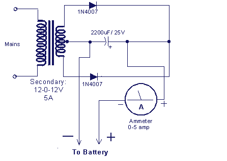
A 12V battery charging circuit is presented, featuring a straightforward diagram for a rectifier. The lead-acid trickle charger circuit is detailed along with its rectifier. The 12V battery charging circuit is designed to charge lead-acid batteries using a trickle charging...
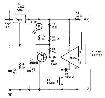
The LM350 car battery charger circuit is a high-performance device designed to efficiently charge gelled lead-acid batteries and automatically terminate the charging process once the battery reaches full charge. This circuit provides a charging current of 2A when the...
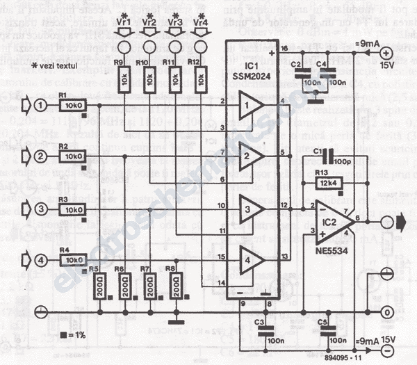
This audio mixer circuit schematic is designed around four current-controlled amplifiers, all integrated within the SSM2024 IC. The audio mixer circuit utilizes the SSM2024 integrated circuit, which features low-noise, high-performance operational amplifiers suitable for audio applications. The SSM2024 is particularly...
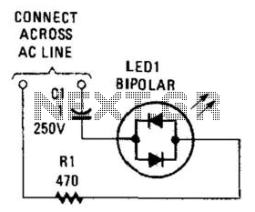
Many electronic circuits require an indication that they are powered. For most AC circuits, a neon lamp is the preferred device. A bidirectional tricolor LED can also be utilized if a capacitor is connected in series with the LED...
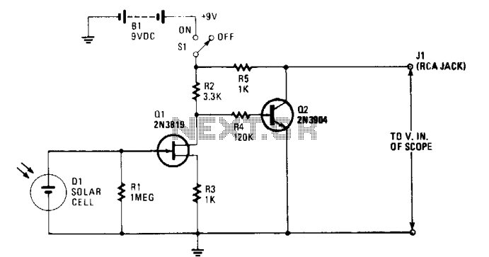
The solar cell is connected to the input of the field-effect transistor (FET), Q1, allowing it to generate a positive DC voltage at the gate when illuminated by light through the open shutter. This illumination reduces the negative gate-source...

This UHF wideband amplifier (Ultra High Frequency amplifier) provides a total gain of 10 to 15 dB in the frequency range of 400 to 850 MHz, making it suitable for areas with weak TV signals. For optimal performance, the...