
Test circuit diagram with feedback factor of 1 83 DA6101Q 6111Q

The DA6101Q/6111Q test circuit is designed for robust signal processing, particularly in applications requiring high fidelity and stability. The input stage utilizes a differential configuration, enhancing the common-mode rejection ratio and improving signal integrity. The feedback network comprising R10 and Cpar plays a crucial role in maintaining the black level, ensuring that the output signal remains stable regardless of variations in the input signal.
The output stage, located at pin 8, is designed to handle transient spikes effectively, offering protection against high-frequency noise and ensuring reliable operation in environments with fluctuating impedance levels. The integration of a bootstrap capacitor (Cn) between pins 7 and 8 is significant for expanding the dynamic range, allowing the circuit to handle a wider range of input signal amplitudes without distortion.
The decoupling capacitors connected to the supply pins (VDDH and VDDL) are essential for filtering out high-frequency noise that could affect the performance of the circuit. The combination of 20nF capacitors with larger 10µF capacitors ensures that the circuit remains stable during operation, particularly under varying load conditions.
Overall, this schematic design is indicative of a well-thought-out approach to signal amplification and processing, making it suitable for applications in video signal processing, high-speed data transmission, and other electronic systems requiring precise signal management. As shown for the test circuit with feedback factor of 1/83 DA6101Q/6111Q is. f input signal input through a network of R1, C1, C2, C3, R9 enter TDA6101Q composed of 3 feet, 3 f eet and 1 foot are the internal differential input stage of the inverting input terminal and inverting input terminal. The amplified signal from the 8-pin output, output through a network of R2, R3, C8, C9 formed to probe.
Between 3 feet and 9 feet resistor R10 and capacitor Cpar feedback network, from the current automatic black level stabilizing role. 8 feet and 7 feet between the resistance and capacitance Cn bootstrap capacitor, the output from the expansion of the dynamic range of action.
Output of 8 feet with a cathode discharge protection. When the high-impedance voltage source to generate a positive spike discharges can withstand 100 C largest capacity 5A current; when the low-impedance source to generate a positive voltage spike discharges can withstand 100nC maximum 10A current capacity. VDDH (6 feet), VDDL (2 feet) must be added decoupling capacitors, decoupling capacitors take 20nF good high-frequency characteristics 10 F ceramic capacitors and electrolytic capacitors connected in parallel.
Related Circuits
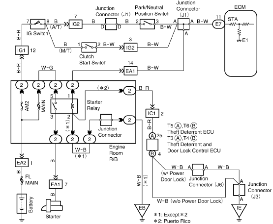
This document provides information regarding the wiring of the Toyota Tercel 1996. Component: intake air temperature sensor. The intake air temperature (IAT) sensor in the 1996 Toyota Tercel plays a crucial role in the vehicle's engine management system. It is...
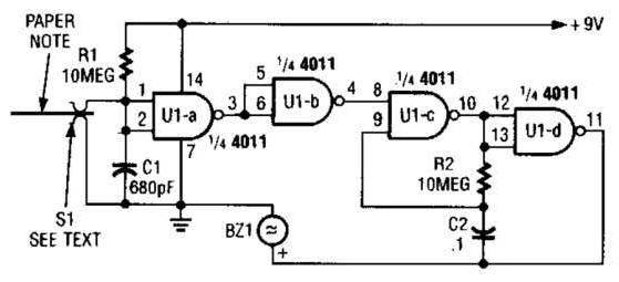
This device prevents paper notes and memos from being overlooked. A paper note placed between two fingers made of a conducting material (metal or conductive plastic) breaks the circuit, allowing pair 1 of Ul-a to go high. The goal...
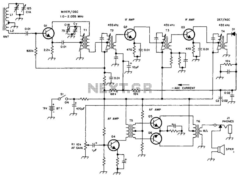
A schematic of a typical transistor AM radio is presented. This circuit utilizes npn transistors. It is a generic circuit; hence, specific values for some components are not provided. This circuit serves as a reference point for experimenters. The schematic...
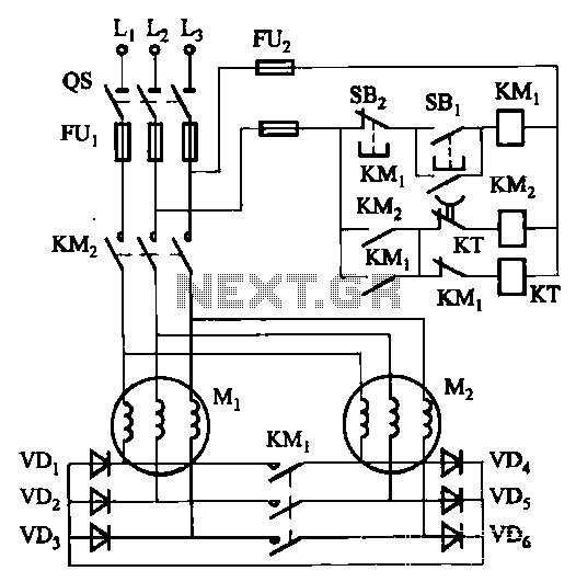
The circuit depicted in Figure 3-157 is designed for motors with a capacity of no more than 11 kW, requiring precise stopping capabilities. Upon shutdown, contact KMi releases, and the motor stator windings are configured into a three-phase rectifier...
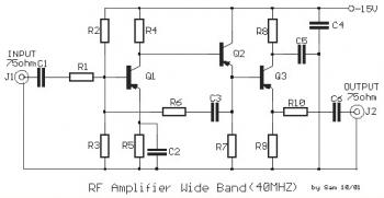
This is a 40 MHz RF amplifier circuit. The sensitivity of a receiver can be significantly enhanced by integrating this circuit between the receiver and the antenna. The amplifier does not utilize resonant circuits and is suitable for both...
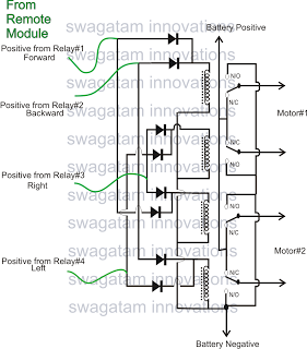
The market is filled with high-end remote-controlled toy cars; however, for hobbyists, creating one at home can be a unique experience. The following article explains how to configure a simple remote-controlled toy car using a pre-made 4-relay remote control...