
Testing Troubleshooting an Inverter Circuit Discussion
Additionally, there was difficulty testing waveforms simultaneously due to limitations of the laptop oscilloscope. Observations of other circuits utilizing the 4017 chip revealed that they do not include buffer transistors; instead, the clock input goes directly to the 4017 and then to the MOSFET gates via a small resistor. It was suggested to experiment with different configurations while keeping a series bulb connected to protect the MOSFETs. After placing 22K resistors across the base and ground of the transistors, a new current draw of 1.80 A was measured, similar to the square wave circuit's 1.82 A. However, the waveform at the gate of the MOSFET driven by IC2 was found to be corrupt, missing a pulse, while the waveform from IC1 was intact. Further checks at the diode junctions confirmed good waveforms.
Recommendations included replacing the transformer with a lower power unit (12V/1 Amp) and testing with smaller loads, such as a 10-watt 120V lamp. Upon testing with a small transformer from an old battery charger, the circuit operated, but the frequency at the gate of MOSFET #2 was over 360Hz, with differing waveforms for MOSFET #1. The transformer was suspected to be the cause of the discrepancies. Future tests will be conducted without the headlight in series, using sacrificial MOSFETs known to work in the original setup.
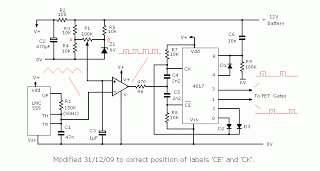
The PWM circuit design aims to control the current draw of an inverter by manipulating the gate drive voltage of the MOSFETs through a buffer transistor arrangement. By integrating variable resistors in the base circuit of each buffer transistor, the voltage supplied to the MOSFET gates can be fine-tuned to optimize performance and reduce excessive current draw. The connection of a lamp and ammeter in series with the inverter allows for real-time monitoring of current consumption, facilitating adjustments to the potentiometer until the desired operational parameters are achieved.
The observed issues during testing highlight the importance of waveform integrity at the MOSFET gates, as any corruption in the signal can lead to inefficient operation or failure to drive the load properly. The comparison of waveforms from different ICs indicates that the configuration of the circuit may need reevaluation, particularly regarding the necessity of buffer transistors, which may not be required based on successful designs utilizing the 4017 chip.
The recommendation to replace the transformer with a lower power model is prudent, as it can help isolate issues related to frequency discrepancies and waveform integrity. Smaller loads should be utilized during testing to prevent damage to components and to ensure safe operation. The analysis of diode junction waveforms further supports the troubleshooting process, indicating that the PWM section may be functioning correctly. The iterative testing approach, including the use of sacrificial MOSFETs, will provide valuable insights into the circuit's performance and guide necessary modifications for optimal operation.Since you say that with my PWM circuit the current consumption of the inverter shoots to a dangerous 14Amps, therefore I just thought, probably we can solve this by reducing the drive voltage to the gates of the mosfets. This can be simply done by controlling the base voltage of the buffer transistors. And that is exactly what we are trying to do by connecting a variable resistor across the base and the ground of each transistor. As discussed earlier, use lamp and ammeter set-up with the inverter and adjust the 15K pot until the current consumption becomes equal to your square wave design. Hi Swagatam, I performed that test with the headlight, Amp meter and PWM circuit, it was drawing 2. 1 Amps, but whenI tried to adjust the Pot, nothing really happened, the Amps did Not increase or decrease, only when i turned the Pot almost all the way left, it would kill the wave form, literly stopping the inverter, then turning the Pot back to the right the wave form would come back and you can hear the inverter run.
The whole time the Headlight did not change in brightness. My laptop Oscilloscope is only Software, with a homemade probe. Unfortunately most laptop Mics Input is in Mono, one channel. So I cant test both wave forms at the same time to see if there overlapping. Another observation I made, Ive been studying a few other circuits that are all using the 4017 Chip. Ive noticed that none of them have those buffer transistors that are used in my original square wave circuit. What ifI remove them from the circuit altogether. Ive noticed that in all the other circuits the Clock Input goes directly to the 4017, then out of the two Outputs that they are using, directly to the gate of the mosfet through a small resistor.
You may try different configurations taking the help of other circuits but always keep the series bulb connected, it will prevent the mosfets from blowing off if something goes wrong. Hi Swagatam, I placed 22K resistors across the base and ground of both transistors, this time when I did the Headlight, Ampmeter to Inverter in series Draw test, I got a readingof 1.
80 A, Exactly the same as the Square Wave circuit, itdrew 1. 82A Now that sounds good, but when I checked the Wave form at the Gateof both banks of Mosfets, the wave form on the Gate that is driven by IC2 is corrupt, it is missing a pulse, Ive sent two screen shots. The screen shot that is missing a pulse comes from the Gate of the Mosfet driven by IC2 and the other screen shot that is not missing a pulse is comes from the Gate of Mosfet driven by IC1.
You will also have to check the waveform at the diode junctions to make sure whether its the fault of the PWM section or is it happening due to the lamp and the base resistor. Replace the present transformer with a much lower power transformer, say a 12-012/1 Amp transformer, after this you may proceed with your waveform checks and also by connecting smaller loads at the output (like a 10watt 120V lamp) and see the results.
Hi Swagatam, I checked the wave form at the diode junctions and the wave form is good there. I have a small transformer out of an old 12V 2Amp battery charger ( not sure if this trans is OK to use for test), and I connected italtogether with No headlight in series. I turn on the circuit and it runsbut when I check the frequency at the Gate of Mosfet #2 driven by IC2 it reads over 360Hz, and the same frequency on the Gate of Mosfet #1 but the wave forms are different, not the same.
I, ve sent you two screen shots. Each shot is labelled accordingly. This has to be happening because of this transformer, I think. What do you think I am going to try the PWM circuit in my Inverter setup without the Headlight in series, with a couple of sacraficial Mosfets I have, that I know work with the Original settup. Ill let you know my results. When you said "I was just thinking to engage the couple of idle gates with the diode junctions " which Id
🔗 External reference
Related Circuits
This circuit diagram illustrates a simple electronic combination lock utilizing the IC LS7220. It is designed to activate a relay for controlling any device (on & off) when a specific combination of four digits is entered. The circuit operates...
This voltage regulator and current limiter combination can be constructed using two 7805 regulators as illustrated. Resistors R1, R2, and R3 should be chosen to achieve a 5-V drop at the maximum allowable current limit. Switch S1 selects one...
A frequency signal tracking circuit is implemented using a phase-locked loop (PLL) configuration, which is a fundamental application of the CD4046 integrated circuit. The circuit, illustrated in the accompanying chart, utilizes the CD4046 to form a PLL that effectively...
It is sufficient to explore PWM (Pulse Width Modulation) and digital-to-analog conversion, illustrating how to create a personal electronics workbench for investigating RC (Resistor-Capacitor) filters, charge and discharge curves, pulse generators, timers, and even a simple oscilloscope to understand...

The transmitter operating at 2 meters (144 MHz) was primarily designed for use by radio amateurs as a radio beacon. It generates a high-quality signal suitable for this purpose. The 2-meter transmitter circuit typically includes several key components to ensure...
This circuit is a 1024 kHz temperature-compensated crystal oscillator. The circuit theory is illustrated. Due to the low output signal level of the circuit, a buffer using the following transistor VT1 is implemented for amplification. The base bias resistor...