
Transformerless Power Supply 30V 1A

This transformerless power supply circuit operates by utilizing capacitive coupling to convert AC voltage to a usable DC output without the need for a transformer. The circuit is particularly suitable for applications requiring medium current levels, typically in low-power devices.
In the operation of the circuit, during the negative half cycle of the AC input, capacitor C5 charges up to the peak voltage present in the AC line. This charging occurs due to the capacitive reactance, which allows current to flow into C5 while blocking DC components. Once C5 reaches its peak voltage, the circuit transitions to the positive half cycle.
As the AC input switches to the positive half cycle, the thyristor is triggered into conduction. This action allows the previously stored charge in C5 to flow into capacitor C4. The transfer of charge from C5 to C4 is crucial, as it provides the necessary energy to power the load connected to the output of the circuit. Capacitor C4 serves as a smoothing capacitor, helping to reduce voltage ripple and provide a more stable DC output.
The design of this transformerless power supply circuit is advantageous in applications where space and weight are critical, as it eliminates the bulkiness of a transformer. However, it is important to note that safety precautions must be taken due to the direct connection to the AC mains, which poses a risk of electric shock. Proper insulation and circuit protection measures should be implemented to ensure user safety and compliance with electrical standards.This transformerless power supply circuit is designed for medium current applications. During the negative half period, the capacitor C5 is charged to peak voltage network. Transformerless Power Supply Circuit Schematic The positive half wave will open the thyristor and the electric charge accumulated in C5 will be transferred in C4. The transport of ele.. 🔗 External reference
Related Circuits
This is a simple non-contact AC power monitor designed for home appliances and laboratory equipment that should remain continuously powered. A failure of the fuse or a power outage in the equipment can lead to significant damage if unnoticed....

The circuit features a serial coded modulated control signal that amplifies and transmits high-voltage isolation. It utilizes a 556 timer-based circuit along with resistors R1, R2, capacitors C1, and R3, R4, C2 to form two astable multivibrators. The circuit...
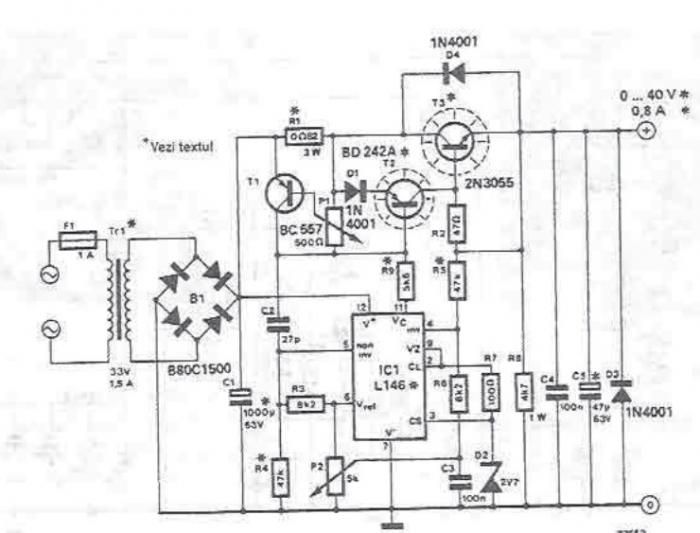
An adjustable laboratory power supply capable of providing an output voltage range from 0 to 60 volts can be constructed using the provided circuit diagram. This power supply can utilize the LM723 chip for lower voltage applications or, for...
This circuit demonstrates that microprocessors, personal computers, and the latest ultra-accurate digital-to-analog converters (DACs) are excessive for the task of sequentially controlling four relays. The circuit utilizes a simple microcontroller or a basic timer IC to manage the operation of...
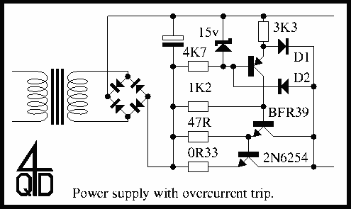
The 15V zener is fed via the 4.7k resistor from the input. With 0.6V across the base-emitter of the PNP transistor, this establishes a voltage of 14.4V across the 3.3k resistor, so there must be a current of nearly...
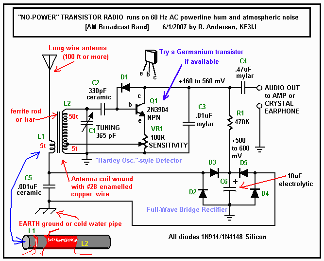
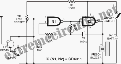
Here is something that may interest crystal radio builders: a one-transistor (silicon) AM broadcast receiver that derives its power from ambient AC hum and static. The schematic is adapted from Darryl Boyd's "Stay Tuned" website, which features over 170...