
Universal multi-function alarm and timer circuit 555

The described multi-function alarm and timing circuit is designed to provide versatile alarm functionalities through a combination of timing and sensor integration. The timing range of 5 minutes to 3 hours allows for flexibility in various applications, making it suitable for both short-term and long-term monitoring tasks. The use of a 555 timer, renowned for its reliability and ease of use, serves as the core timing mechanism.
The circuit configuration includes a capacitance multiplier, which enhances the effective capacitance seen by the timing circuit, thereby improving stability and response time. The input voltage of approximately 9V DC from CK1 is critical for the operational integrity of the circuit, particularly in radio applications where consistent timing is essential.
The activation of K1 allows for user-defined timing adjustments, enabling the circuit to cater to specific requirements. The 555 timer output, which ranges from 6V to 9V, indicates the readiness of the circuit to activate alarm functions. The transition of pin three from high to low upon timer expiration is a pivotal moment in the circuit operation, as it initiates the deactivation of CK1 and the subsequent activation of VT2.
The alarm circuit, comprising components F1 and F2, is designed to emit both sound and light signals for a specified duration of 20 seconds, ensuring that the alarm condition is effectively communicated. The additional outputs F3 to F5 provide further alarm functionalities, allowing for a comprehensive alert system. Furthermore, the capability to integrate various sensors on both sides of the circuit enhances its adaptability, enabling customization based on specific monitoring needs. This design exemplifies a robust solution for alarm and timing applications, combining ease of use with extensive functional capabilities. As shown for the general multi-function alarm and timing circuitry. The timing of the circuit can range from 5 minutes to 3 hours. Timing components C2, VD1 and VT1 composition capacitance multiplier circuit 555. CK1 from the timing input socket ~ 9V DC voltage, and so the timing for radio work. K1 is set to the timing gear, press the AN, 555 feet high output (6 ~ 9V), while VT2 off. When the timer expires, the three 555 pin goes low, CK1 no voltage output, VT2 is turned on, the alarm circuit F1 and F2 generation of the alarm sound and light alarm 20 seconds and F3 to F5 generated. A, B-side can add a variety of additional sensors sound and light alarm circuit.
Related Circuits
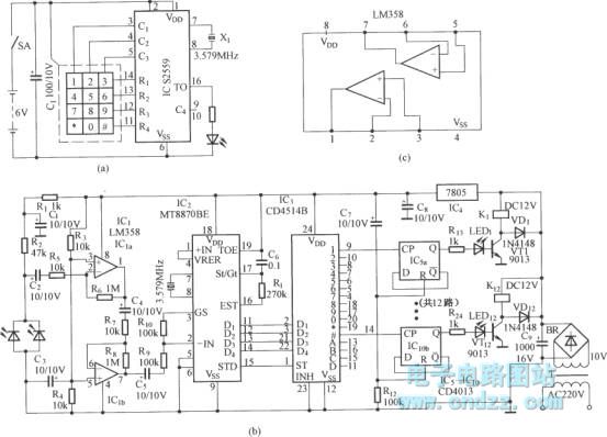
Figure (a) illustrates an infrared emission circuit composed of a 12-key keyboard and an S2559. Figure (b) displays a DTMF decoder circuit along with a channel control circuit utilizing the MT8870. Figure (c) presents a voltage amplifier circuit constructed...
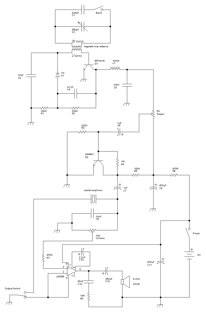
This receiver is a modification of Charles Wenzel's Two Transistor Reflex Radio. Instead of a ferrite AM loopstick antenna, a magnetic loop antenna is used, and an LM386 amplifier stage has been added to drive an 8-ohm speaker. A...
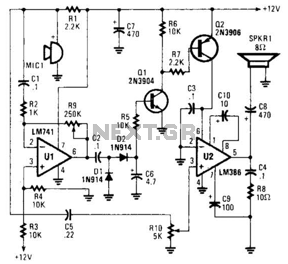
An omnidirectional electret microphone is utilized to capture sound and convert it into an electrical signal. The output from the microphone is directed along two pathways. In the first pathway, the signal is routed to the inverting input at pin...
An oscillator is a mechanical or electronic device that operates based on the principles of oscillation. Oscillators serve as fundamental building blocks upon which the entire structure of electronics and computers is established. An article is available that explains...

A transistor optocoupler interface circuit, as described in section 15.1.6, has been implemented. This circuit serves as a transistor interface with other circuits. The transistor optocoupler interface circuit utilizes a light-emitting diode (LED) and a phototransistor to achieve electrical isolation...
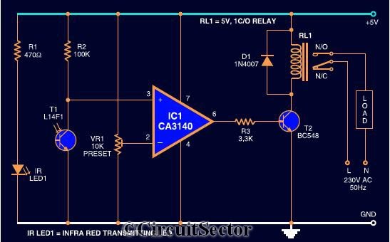
The circuit diagram presented is a highly sensitive wireless relay switch designed to control home appliances such as flush systems and hand dryers. This wireless switch operates without the need for a remote control. It functions by simply moving...