
Unsteady direct coupling circuit diagram

In this circuit configuration, the direct coupling of the collector and base-emitter bias establishes a feedback mechanism that enhances the performance of the transistors. The triangular wave generated by the emitter serves as a modulation signal, which is essential for applications requiring signal processing or waveform generation.
The operation of the circuit is characterized by its ability to switch between two distinct states. These states correspond to the charging and discharging phases of the capacitive elements in the circuit. During the charging phase, the circuit allows current to flow into the capacitors, storing energy. Conversely, during the discharging phase, the stored energy is released, facilitating the conversion of electrical energy.
The design of this circuit is particularly useful in applications such as signal modulation, where the triangular wave can be used to create varying voltage levels that can be transmitted or processed further. Additionally, the ability to switch states efficiently enables the circuit to conserve power, as the transistors are not continuously active, reducing thermal dissipation and enhancing overall reliability.
The implementation of such a circuit requires careful consideration of component values, including the resistors and capacitors, to ensure the desired frequency and amplitude of the triangular wave are achieved. Moreover, the selection of transistors with appropriate characteristics is crucial to optimize performance and efficiency in the intended application. Overall, the described circuit offers a robust solution for applications requiring effective signal modulation and energy conversion. Both collector and base-emitter bias transistor is coupled directly to each other. Each transmitter circuit capacity control conversion function. The emitter generates a triang ular wave. Two transistors are not always kept awake state. In contrast, the circuit has two fixed state, between these states charge and discharge capacity can be achieved conversion.
Related Circuits
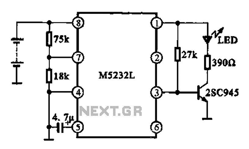
A battery voltage indication circuit that changes the status display. When the battery voltage is normal, an additional transistor drives an LED, which remains off. However, if the battery voltage falls below a critical threshold, the LED begins to...
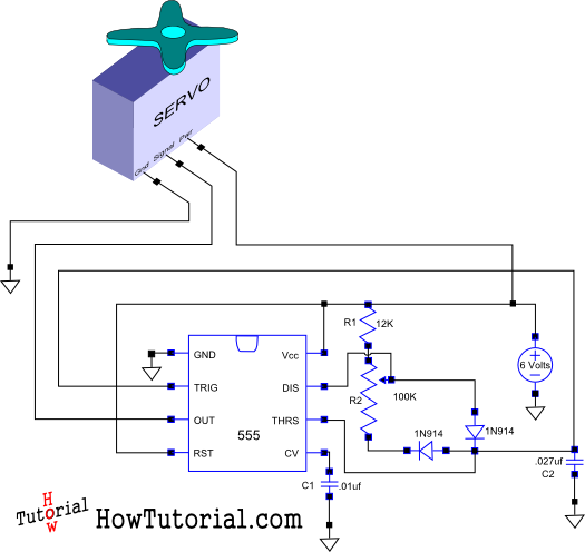
This document outlines the design of a simple circuit that enables control of a servo motor and allows for testing its functionality. The circuit for controlling a servo motor typically consists of a microcontroller, a power supply, and the servo...
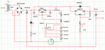
This circuit consists of two main components: a battery charger that provides a fixed output voltage of 5V DC, and a regulated power supply that allows for an adjustable output voltage ranging from 2 to 9 volts. The circuit design...
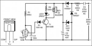
The following circuit illustrates an IR Remote Control Tester Circuit. Features include that transistor T1 conducts during the negative pulse period, and there is a data output pin. The IR Remote Control Tester Circuit is designed to verify the functionality...

This field strength meter consists of a tuned crystal detector that generates a DC output voltage from a transmitted signal. The DC voltage is utilized to modulate the frequency of a transmitter with a power output of 100 mW,...
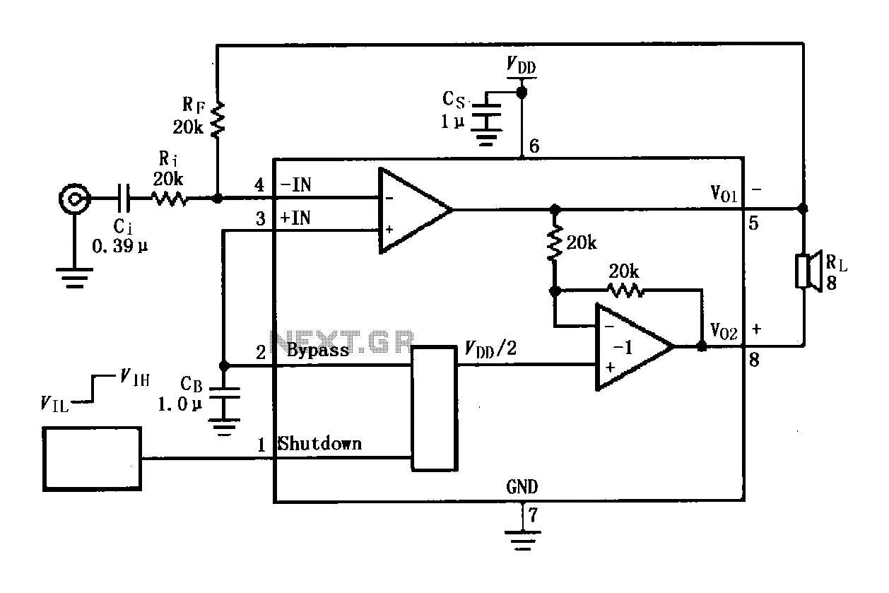
The LM4819 audio power amplifier is designed to amplify audio signals. An audio signal is input through the coupling capacitor (Ci) and the resistor (Ri) applied to the inverting input terminal (pin 3) of the amplifier. The inverting input...