
usb cellphone charger circuit

The USB cellphone charger circuit is designed to convert AC mains voltage into a stable DC voltage suitable for charging mobile devices. This circuit typically utilizes a transformer, a rectifier, a voltage regulator, and various passive components to ensure efficient operation and safety.
The primary component, the transformer, steps down the high AC voltage from the mains to a lower AC voltage, which is then fed into a rectifier circuit. The rectifier, usually composed of diodes arranged in a bridge configuration, converts the AC voltage into pulsating DC. Following the rectification process, a filter capacitor is employed to smooth the pulsating DC output, reducing voltage ripple and providing a more stable voltage.
To regulate the output voltage to the desired level (commonly 5V for USB charging), a voltage regulator is integrated into the circuit. This component ensures that the output voltage remains constant despite variations in load or input voltage. Commonly used voltage regulators for USB applications include the LM7805 for linear regulation or switching regulators for improved efficiency.
Additional components such as resistors, capacitors, and possibly a fuse are included to enhance circuit performance, provide noise filtering, and protect against overcurrent conditions. The circuit design may also incorporate protection features such as a diode to prevent reverse polarity and a surge protector to safeguard against voltage spikes.
The final output is typically connected to a USB port, allowing for compatibility with various mobile devices. The design may vary depending on specific requirements, such as output current capacity and efficiency considerations. Overall, the USB cellphone charger circuit is a practical and essential design in modern electronics, providing a reliable means to charge portable devices.Good information about USB Cellphone Charger Circuit You can learn and download USB Cellphone Charger Circuit online here.. 🔗 External reference
Related Circuits
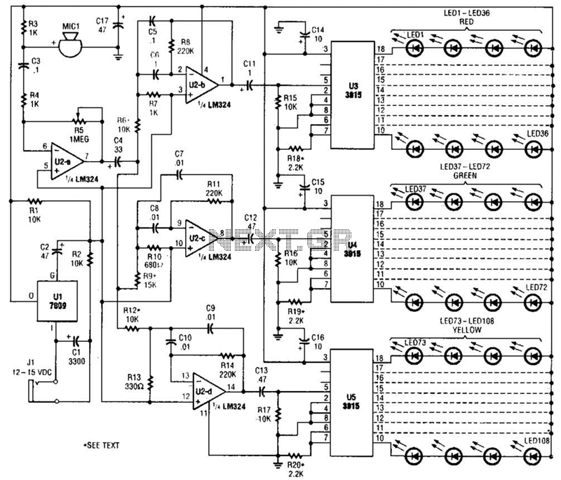
The microphone input, MIC1, is connected through capacitor C3 and resistor R4 to the inverting amplifier U2-a, where the gain of U2-a is adjusted by potentiometer R5. The output from U2-a is passed through capacitor C4 to the remaining...
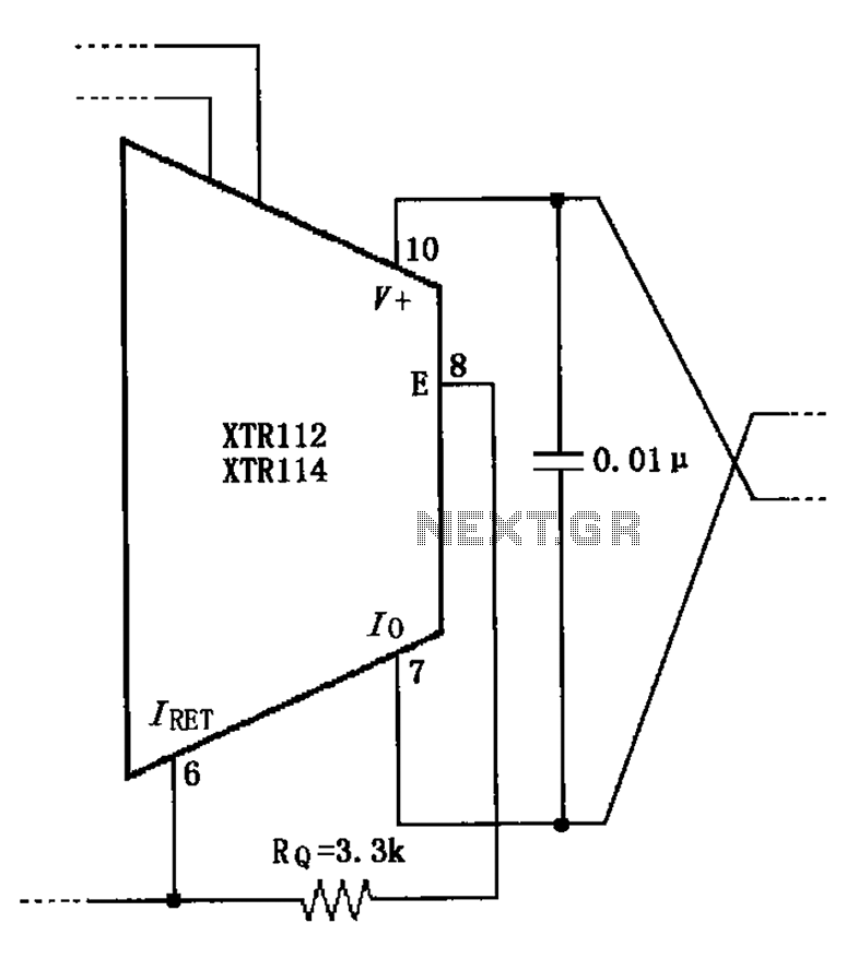
When not using the external transistor Q1, a 3.3k resistor should be connected between the pins and legs. This connection causes internal power dissipation, which will affect accuracy and lead to a decline in performance. The circuit in question involves...

The TDA6106Q test circuit, as depicted in the provided figure, operates with a feedback factor of 1/116. The input signal, Vin, is received from the input network consisting of resistors R1, R9 and capacitors C1, C2. The TDA6106Q IC...
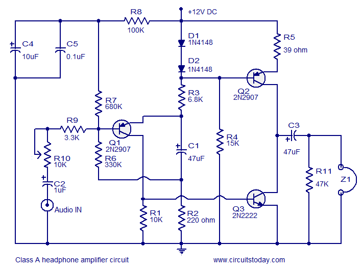
Transistor amplifier circuits that are simple and easy to construct. This includes a headphone amplifier, a four-transistor amplifier, and a low-power amplifier. Transistor amplifier circuits are fundamental components in electronic design, offering various applications ranging from audio amplification to signal...

The 555 timer generates a rapid series of pulses when switch SI is in the open position. These pulses are grouped into sets of 16 and converted into binary format by the 7493 counter. The binary output is then...
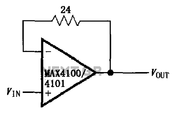
The circuit illustrated is a unit gain buffer circuit utilizing the MAX4100/4101 operational amplifiers. It incorporates a small resistor (24 ohms) within the feedback loop of the amplifier, thereby establishing a unity gain buffer. This configuration maximizes the bandwidth...