
voltage conversion circuit composed of VFC320

The circuit in Figure 1-22 (a) utilizes a voltage-to-frequency converter (VFC), specifically the VFC320, which is designed to generate a frequency output proportional to the input voltage. The input voltage is applied to the VFC320, which modulates the output frequency based on the input signal. The output frequency can be adjusted by changing the values of the resistors and capacitors in the circuit. The connection of pin 7 to a resistor enables the output to interface seamlessly with standard digital logic circuits, allowing for further processing or control applications.
In Figure 1-22 (b), the circuit takes a pulse input with a frequency range of 0 to 100kHz and converts it back into a corresponding output voltage ranging from 0 to +10V. This conversion is typically achieved using a frequency-to-voltage converter (FVC), which processes the incoming pulse signal and generates a DC output voltage that is proportional to the frequency of the input pulse. The output voltage can be fine-tuned using additional components in the circuit, such as operational amplifiers or voltage dividers, to ensure compatibility with various applications that require a specific voltage range.
Overall, both circuits exemplify the versatility and functionality of voltage and frequency conversion in electronic applications, enabling seamless integration between analog and digital systems.Figure 1-22 (a) shows the circuit which could convert 0-+lOV input voltage Ui into the pulse with 0 -1OOkHz output frequency, and pin 7 of VFC320 is connected a resistor to directly connect to standard logic. Figure 1-22 (b) shows the the circuit which could convert the pulse with 0-100KHz input frequency into 0-+lOV output voltage UO.
If the signal counter.. 🔗 External reference
Related Circuits
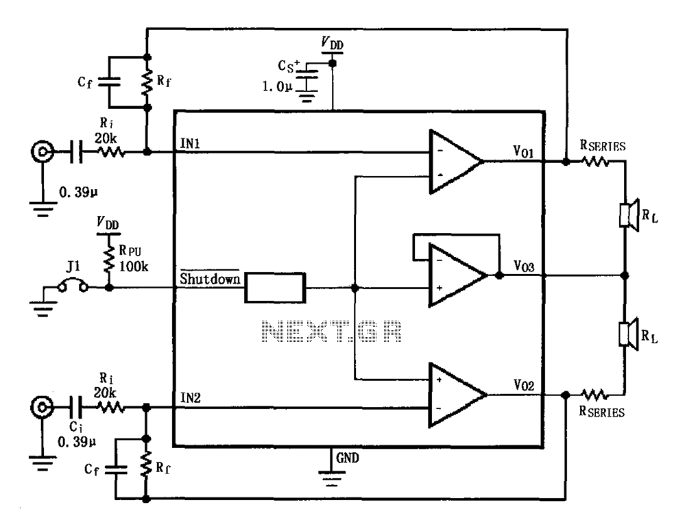
The circuit for the LM4910 is designed to minimize output noise and reduce power consumption. The output noise is attenuated by utilizing a resistor in series with the load. A feedback resistor Rf is used in conjunction with a...
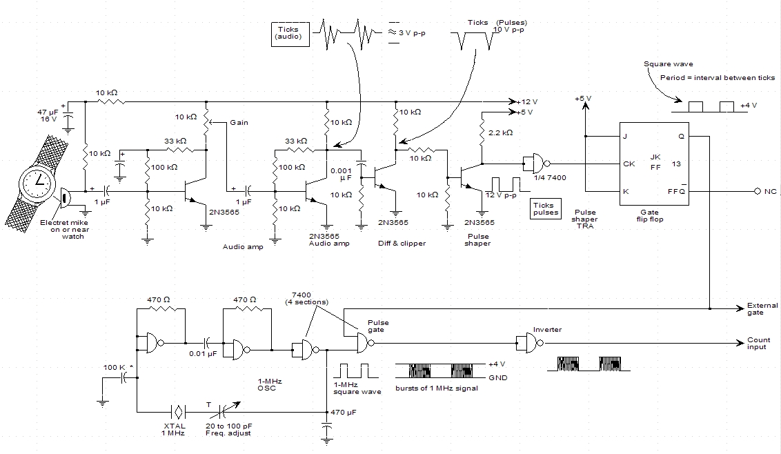
A schematic for a watch timer was found in a hobby electronics book. The circuit adapts a frequency counter to measure intervals. Watch ticks are clipped, shaped, and formed into a square wave. This square wave is utilized to...
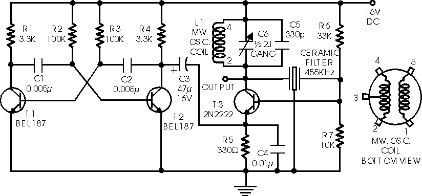
This is a range of IF signal circuits that may be of interest to radio hobbyists and professionals alike. Transistors T1 and T2 form an astable multivibrator oscillating in the audio frequency range of 1 to 2 kHz. An...
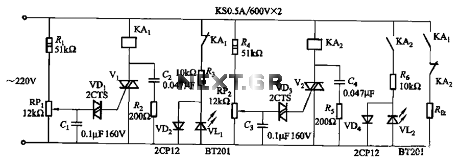
Bidirectional thyristor control. By adjusting potentiometers RPi and RPz, the lower and upper limit values can be changed. LEDs VLi and VL2 serve as indicators for low pressure and high pressure, respectively. The circuit utilizes a bidirectional thyristor to control...
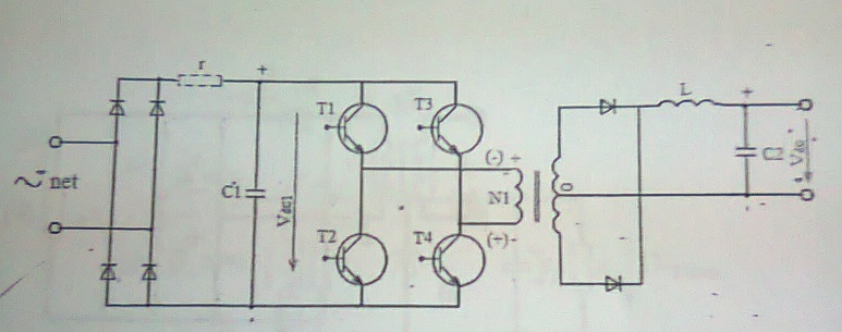
A power supply with frequent energy switching; however, the schematic is incomplete. An additional circuit is needed to control the voltage polarity converter, which consists of four transistors. This circuit generates high-frequency current pulses. Assistance is appreciated to explain...
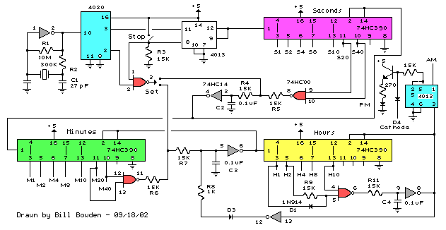
This device is a combination digital clock timer and solar panel charge controller designed to maintain a deep cycle battery from a solar panel. The timer output controls a 12-volt load for a 32-minute interval each day. The start...