
Welder no-load power saver circuit diagarm 5

The welder no-load power saver circuit is designed to minimize energy consumption when the welder is not actively engaged in welding tasks. The current detection control circuit plays a crucial role in monitoring the current flowing through the welder. The current transformer (TA) is employed to sense the current and convert it into a proportional lower current suitable for processing.
The bridge rectifier (UR) converts the alternating current (AC) output from the current transformer into direct current (DC). This DC signal is then filtered and stabilized using the resistor (R1) and the Zener diode (VS), ensuring that the voltage remains within a specified range. The capacitor (C2) serves to smooth out any fluctuations in the rectified voltage, while the diode (VD) protects the circuit from reverse polarity.
The power saving control circuit is responsible for regulating the power supplied to the welder during idle periods. By utilizing resistors in this circuit, the system can effectively limit the power draw, thereby reducing overall energy consumption. This circuit operates in conjunction with the current detection control circuit to ensure that power is only consumed when necessary, thus enhancing the efficiency of the welder.
Overall, the welder no-load power saver circuit is an essential component for modern welding equipment, contributing to energy efficiency and operational cost savings. Its design incorporates various electronic components that work together to detect current usage and regulate power consumption, thereby providing a sustainable solution for welding applications.The welder no-load power saver circuit is composed of the current detection control circuit and power saving control circuit, and the circuit is shown as the chart. Current detection control circuit is composed of the current transformer TA, bridge rectifier UR, resistor R1, Zener diode VS, capacitor C2 and diode VD.
Power control circuit consists of resisto.. 🔗 External reference
Related Circuits

The following circuit illustrates a Bedside Lamp Timer Circuit Diagram. This circuit is based on the CD4060 integrated circuit. Features: An LED illuminates for approximately 25 seconds. The Bedside Lamp Timer Circuit utilizes the CD4060 IC, which is a versatile...
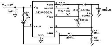
The ADM666A application note provides a detailed explanation of a low-cost battery charger circuit, including maximum output voltage, charge termination voltage calculation, battery voltage level monitoring, and circuit efficiency optimization. The ADM666A utilizes an NPN transistor and a P-channel...
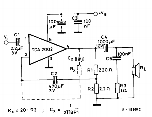
This is a power amplifier circuit built using the TDA2002 power amplifier IC module. It serves as a replacement for the original LM383, which is no longer available. The circuit is easy to assemble and requires a minimal number...
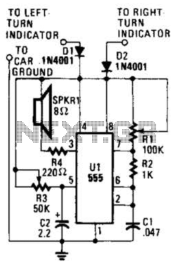
This circuit is designed to assist individuals with hearing impairments by generating a tone each time a dashboard turn indicator is activated. The frequency of the tone decreases for the duration that the indicator remains lit. The circuit operates by...
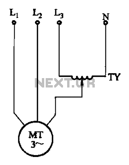
The circuit illustrated in Figure 3-175 features a regulator connected between one phase and neutral. It is designed for use with a 380V torque motor. This method offers advantages over the serious line imbalance approach, resulting in improved operating...
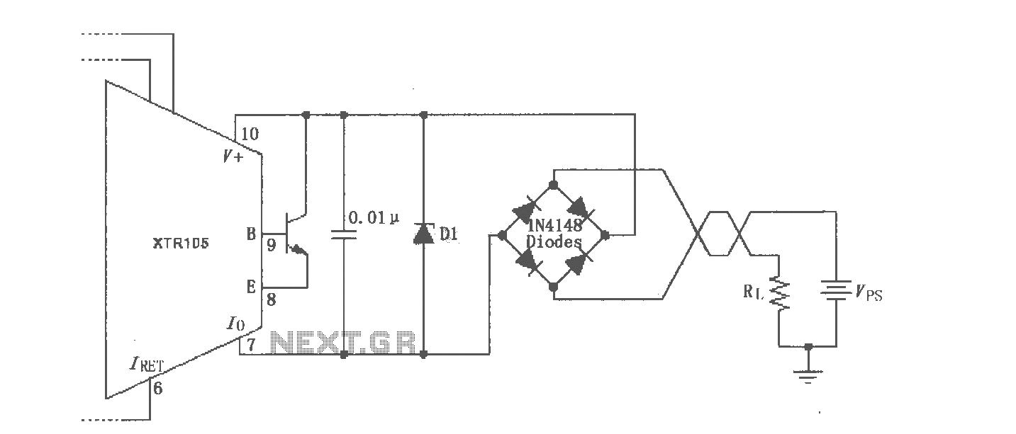
The XTR105 reverse voltage and over-voltage surge protection circuit is illustrated. A Zener diode rated at 36V can be utilized, with options including 1N4753A or 1N6286A. The maximum supply voltage (Vps) should be less than the minimum breakdown voltage...