
12V High current regulator
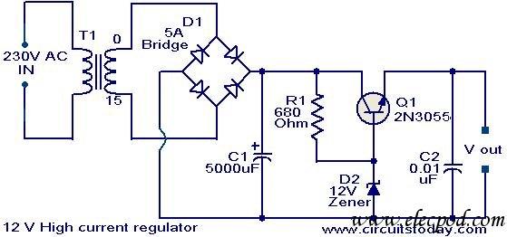
The voltage regulator circuit described is designed to provide a reliable output voltage of 12V with a current capacity of up to 3A. This is particularly useful in applications requiring stable power supply under variable load conditions. The circuit begins with transformer T1, which is responsible for stepping down the high-voltage AC mains supply to a lower voltage of 12V RMS. This is a critical first step in ensuring that the subsequent components operate within their safe voltage ratings.
The rectifier bridge D1, composed of four diodes arranged in a bridge configuration, converts the stepped-down AC voltage into pulsating DC. This pulsating DC is then smoothed out by capacitor C1, which acts as a filter to reduce voltage ripple, providing a more stable DC voltage output. The value of C1 is chosen based on the expected load current and the desired ripple voltage, ensuring that the output remains as steady as possible under varying load conditions.
The core of the voltage regulation is achieved through the use of the series pass transistor Q1, specifically the 2N3055 model. This transistor is capable of handling high currents, making it suitable for this application. The biasing of Q1 is accomplished through resistor R1, which sets the base current necessary for the transistor to operate in its active region. The zener diode D2 is crucial for maintaining the output voltage at a constant level. When operating in its breakdown region, D2 clamps the voltage across it to 12V, ensuring that the base voltage of Q1 remains stable.
The output voltage is theoretically calculated to be 11.3V, which accounts for the voltage drop across the base-emitter junction of Q1. This slight reduction from the zener voltage is important to note, as it impacts the overall performance of the voltage regulator. As the load current increases, Q1 will conduct the excess current, allowing the circuit to maintain the output voltage as specified. This design is particularly advantageous for applications that require a robust power supply capable of handling transient loads without significant voltage fluctuations.
Overall, this voltage regulator circuit is an effective solution for providing a stable 12V output at currents up to 3A, utilizing readily available components to achieve reliable performance in various electronic applications.This voltage regulator circuit can deliver up to 3A at 12V output voltage. The circuit can be employed on occasions when a current of more that 3A is demanded for regulator. IC regulators of such high current rating are pretty hard to find. The transformer T1 steps down mains voltage, to 12rms & the rectifier bridge D1 rectifies it to produce a DC voltage. The C1 filters the rectifier output and produces a DC level. The series pass transistor Q1 (2N 3055) is biased by resistor R1 (680 ). Since zener diode D1 is under breakdown region the voltage across it will be 12V. So the total output voltage will be steady 11. 3 V(theoretically). That is the zener voltage minus base emitter voltage of Q1. Here transistor Q1 will conduct the excess current required. 🔗 External reference
Related Circuits
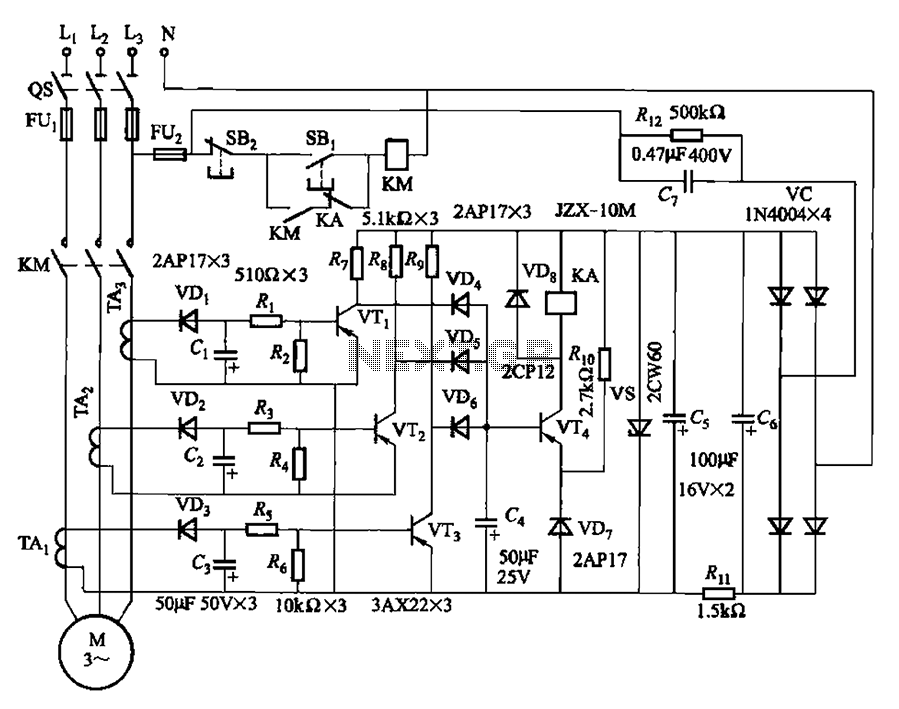
The current detection signal is obtained from three current transformers after rectification and filtering, resulting in three DC voltage outputs. These voltages are applied to transistors VT1, VT2, and VTa between the base and emitter. The signal is amplified...
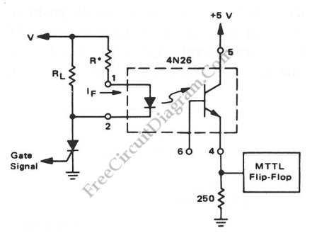
Interfacing high power loads can be accomplished in various ways, including the use of voltage divider resistors, transformers, or optocouplers. The circuit illustrated below employs the optocoupler method. This optocoupler facilitates logic level translation with flexible input, accommodating a...
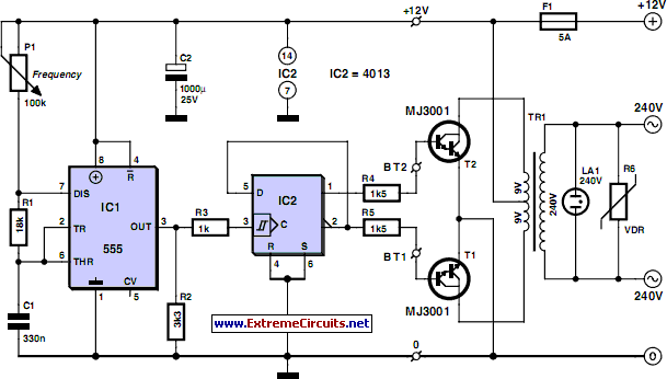
Although modern electrical appliances are increasingly self-powered, particularly portable devices used during camping or summer vacations, there are still occasions when a 230 V AC source is necessary. Additionally, it is beneficial for this source to operate at a...
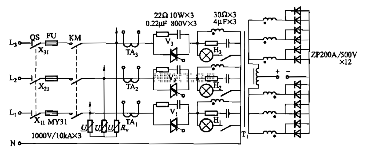
A 1500A-7V phase thyristor power regulator circuit is designed for plating applications. It consists of three major components: the main circuit, the control circuit, and the protection circuit. The control circuit includes a trigger circuit, a synchronous power supply,...

A step-up converter can be designed using the MAX641 integrated circuit from Maxim IC, utilizing a minimal number of electronic components. This high-voltage step-up converter project can deliver a maximum output current of up to 1A. The low battery...

A filter removes the DC component of the rectified AC, which is then scaled to RMS. The output is linear from 40 Hz to 10 kHz or higher. The described circuit primarily consists of a filter designed to eliminate the...
Warning: include(partials/cookie-banner.php): Failed to open stream: Permission denied in /var/www/html/nextgr/view-circuit.php on line 713
Warning: include(): Failed opening 'partials/cookie-banner.php' for inclusion (include_path='.:/usr/share/php') in /var/www/html/nextgr/view-circuit.php on line 713