
250mw 16 db vhf amplifier
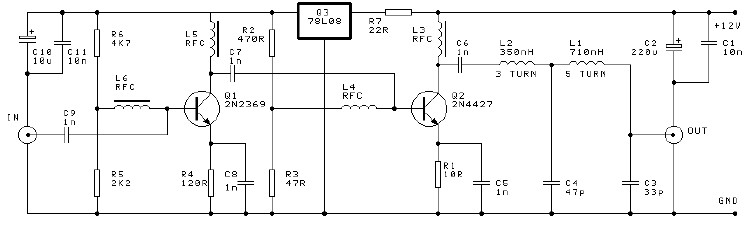
The 250mW RF power amplifier circuit is structured around two transistors configured in a push-pull arrangement to enhance efficiency and output power. The choice of components is critical; transistors with suitable frequency response and power handling capabilities are selected to ensure optimal performance in the VHF range. The circuit is designed to operate within the frequency range typically used for FM broadcasting, which is between 88 MHz and 108 MHz.
The amplifier circuit exhibits a significant gain of approximately 16dB, which allows for the effective amplification of the relatively low output power from wideband FM transmitters. The use of wideband techniques ensures that the amplifier maintains consistent performance across the entire operational bandwidth, minimizing distortion and maximizing fidelity.
To further enhance the quality of the output signal, a low-pass filter is integrated into the design. This filter is essential for removing unwanted harmonic frequencies generated during amplification, thereby ensuring that the output signal maintains good spectral purity. The inclusion of this filter not only improves the quality of the transmitted signal but also helps to comply with regulatory standards regarding spectral emissions.
The layout of the circuit is optimized for assembly on a single-sided printed circuit board (PCB), which simplifies the manufacturing process and reduces production costs. The PCB design minimizes the length of signal paths, which is important for maintaining signal integrity and reducing potential interference. Careful attention is given to the placement of components to ensure proper thermal management and to prevent signal degradation.
In summary, this RF power amplifier project is a well-engineered solution for amplifying the output of low-power wideband FM transmitters. Its design incorporates effective amplification techniques, filtering for spectral purity, and considerations for practical assembly, making it a reliable choice for applications requiring increased RF output power.This is an 250mW RF power amplifier project. This circuit is designed to amplify the output of about 7mW wide band FM transmitters to a final level of about 250mW. This electronic circuit is a simple 2-transistor VHF power amplifier, with about 16dB gain, and requires no tuning or alignment procedures.
Wideband techniques have been used in the design and the circuit is equipped with a lowpass filter to ensure good output spectral purity. The project has been designed for assembly on a single-sided printed circuit board. The circuit is specifically designed to amplify the output of 7mW to 10mW WBFM transmitters (wide band) to a final level of 250mW to 300mW, after the filter. 🔗 External reference
Related Circuits
The 20-W + 20-W stereo amplifier consists of two complete, separate 20-W RMS bridge-type amplifiers. The input signal source is brought into the amplifier through a voltage divider network, which is composed of resistors R1, R2, and potentiometer P1....
This balanced preamplifier circuit is designed to amplify low-level audio signals (from 0 dB to 20 dB) and features balanced inputs and outputs. The design utilizes standard components that are readily available in the electronics market. The balanced preamplifier circuit...
The three stages commonly found in audio amplifiers and operational amplifiers are clearly visible. However, actual audio designs often feature modifications and enhancements in key areas. This overview highlights design improvements in audio amplifiers, focusing on each of the...
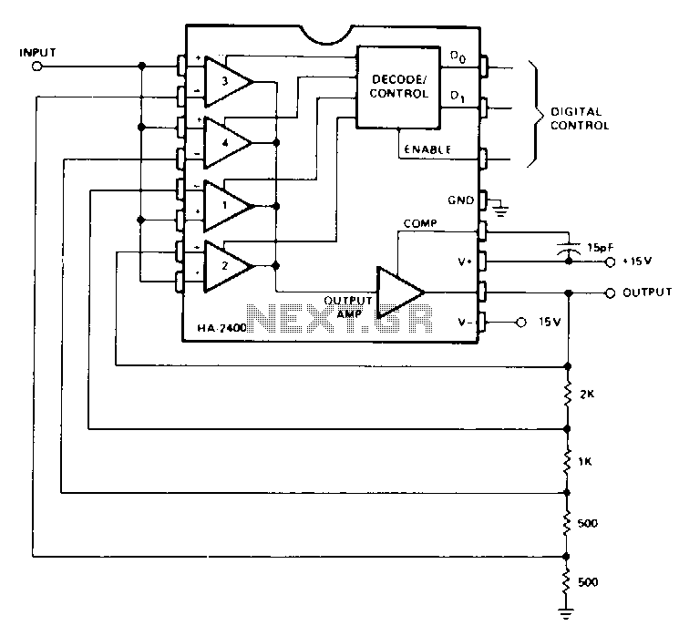
This is a non-inverting amplifier configuration with feedback resistors selected to achieve a gain of 0, 1, 2, 4, or 8, based on digital control inputs. Comparators at the output may be utilized for automatic gain selection in applications...

In an audio amplifier, the quality of sound depends on several factors, including the quality of active and passive components, circuit configuration, and layout. The selection of components is influenced by the constructor's budget. Discrete active components like transistors...
The schematic illustrates the subwoofer amplifier stage, specifically the pre-amplifier circuit and the signal processing circuit. Notably, it features two LM3886 power ICs from the American company NS, which facilitate BTL (Bridge-Tied Load) speaker operation at an 8-ohm impedance...
Warning: include(partials/cookie-banner.php): Failed to open stream: Permission denied in /var/www/html/nextgr/view-circuit.php on line 713
Warning: include(): Failed opening 'partials/cookie-banner.php' for inclusion (include_path='.:/usr/share/php') in /var/www/html/nextgr/view-circuit.php on line 713