
400-Volt 60-watt push-pull power supply
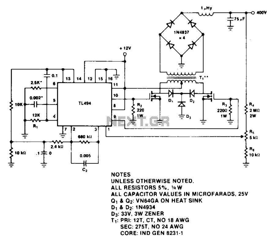
The circuit employs the TL494 integrated circuit, which is a versatile PWM controller capable of regulating high voltages efficiently. The output voltage of 400 V is achieved through a combination of switching techniques and feedback control. The operating frequency is determined by the values of R1 and C1, which are critical for setting the desired frequency range, allowing the circuit to adapt to different load conditions.
The FETs are driven directly by the TL494, ensuring rapid switching and minimizing losses associated with slower gate drive techniques. This results in improved efficiency and thermal management, essential for high-power applications. The full-wave rectification stage converts the AC output from the transformer into a DC voltage, which is then smoothed by the choke-input filter. The combination of the 1 µF and 75 µF capacitors provides effective filtering, reducing voltage ripple and ensuring stable output.
The feedback network consisting of resistors R4, R5, and R6 is designed to monitor the output voltage and adjust the PWM signal accordingly to maintain the desired voltage level. Capacitor C2 serves as a loop compensation element, stabilizing the feedback loop and enhancing transient response. The inclusion of diodes D1 and D2 ensures that the output remains isolated from voltage spikes and transients, while the zener diode D3 clamps excessive voltage, protecting sensitive components from overvoltage conditions.
The overall design achieves a high level of output voltage regulation, with a deviation of only 1.25% across the full load range. This precision is crucial in applications where voltage stability is necessary for the proper functioning of downstream circuitry. The output noise and ripple, primarily consisting of switching spikes, are kept within acceptable limits, ensuring reliable operation in various electronic environments. This design exemplifies a robust approach to high-voltage power regulation, suitable for demanding applications.The design delivers a regulated 400-V, 60-W output. The TL494 switching regulator governs the operating frequency and regulates output voltage. Rl and Cl determine switching frequency, which is approximately 0.SRC—100 kHz for the values shown. The TL494 directly drives the FET's gates with a voltage-controlled, pulse-width-modulated signal. After full-wave rectification, the output waveform is filtered by a choke-input arrangement. The 1 µ, 75 µ¥ filter accomplishes the job nicely at 100 kHz. A feedback scheme using R4, R5 and R6 provides for output-voltage regulation adjustment, with loop compensation handled by C2. Diodes Dl and D2 provide isolation and steering for the 33-V zener transient clamp, D3. Output regulation is typically 1.25% from no-load to the full 60-W design rating. Regulation is essentially determined by the TL494. Output noise and ripple consists mainly of positive and negative 0.8-V spikes occurring when the output stage switches.
🔗 External reference
Related Circuits
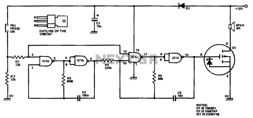
ICla and IClb are configured as a slow astable multivibrator, while IClc and ICld are arranged as a fast astable multivibrator. The output from the slow astable modulates the frequency of the fast astable, and the output from the...
This circuit allows appliances to remain connected to an inverter. While it does not influence weather conditions, it ensures that batteries are safely charged even during periods of generation shortfall. This device is referred to as the Grid Charger...
The device shows a voltage of 24V at no load on pins +4, 5 and -7, 8. This configuration is referred to as a passive power injector. When a current draw of 1A was attempted from the device, it...
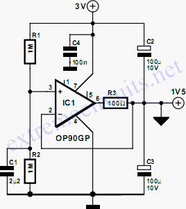
Many modern circuits operate from a single supply voltage of 3V. However, they often require a virtual ground at half the supply voltage for optimal performance. The splitter depicted in the diagram divides the supply voltage using a high-resistance...
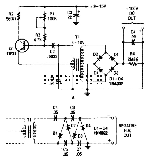
The combination of a Hartley oscillator and a step-up transformer can generate significant negative high voltage, particularly when the voltage output of the transformer is multiplied by the circuit in B. The Hartley oscillator is a type of LC oscillator...
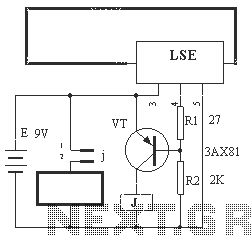
The circuit operation principle of the device illustrated in Figure 13 is as follows: When the barbed wire (Fe) remains intact, the output pin (O) of the LSE is at a high state. Consequently, the transistor (VT) remains off,...