
472 kHz Transmitter

The exciter board's architecture is crucial for achieving reliable operation in RF applications. The integration of a DDS module allows for precise frequency generation, essential for WSPR (Weak Signal Propagation Reporter) communications. The choice of a Class-E amplifier topology is particularly advantageous due to its high efficiency and ability to handle significant power levels, making it suitable for amateur radio applications. The use of a CMOS 4069 for waveform shaping is a common practice, allowing for the generation of a square wave necessary for driving the FET effectively.
The transition to bipolar transistors for the driver circuit indicates a focus on improving the rise and fall times of the output signal, which is critical for maintaining signal integrity and minimizing distortion in high-frequency applications. The design of the low-pass filter as a 5th order Chebyshev filter demonstrates an understanding of the need for harmonic suppression in RF amplifiers, ensuring that unwanted frequencies are attenuated before transmission.
The PCB design process highlights the iterative nature of electronic development, where multiple revisions are often required to refine performance. The inclusion of air-core inductors and high-quality capacitors in the LPF design reflects a commitment to using components that can withstand the operational stresses of high-power applications.
In summary, the described exciter board and associated power amplifier represent a well-thought-out design aimed at achieving efficient and reliable performance in amateur radio transmission, with careful consideration given to component selection, circuit design, and filtering techniques.The exciter board is based on my Arduino WSPR exciter. I do plan to create a better stand-alone board soon, with one of these Chinese DDS modules that are cheap and easy to get from eBay. At the minute I am using a DDS60 by AmQRP. The output from this amplifier is small (around 980mV unloaded, about 290mV into 47 ©). The scope trace below shows w hat the DDS-60`s output looks at 472 kHz. The sinewaves are a little flat-topped but this doesn`t matter as it`s only at the driver stage. The PA will be class-E and so will completely distort the signal and require cleaning later. My first power amplifier was closely based on GW3UEP`s 25W PA. I adjusted some of the coil inductances and altered the design fractionally to better suit what I had, but it is still in essence GW3UEP`s design. From the input waveform above, I have used a CMOS 4069 with one of the input gates biased half on to convert the input into a square wave to drive the FET.
I used a very crude circuit: At the output of the Sine-to-TTL converter, there is a square-wave pulse train at the input frequency. This signal is fed to the FET gate, which is where this voltage train was measured. Left is the time domain, right the frequency domain via fast Fourier transform. The drive on the FET`s gate is amplified. The drain of the FET has the amplified signal. The two images below show the time and frequency domain on the drain. Finally, here we can see the filtered sine-wave output and FFT from the PA. I`m still not happy with the design, it needs a little more filtering, and a little more harmonic suppression, which is why it`s still not been on air yet.
13. 18 Watts dissipated into the 47 © (47 is what I had) (See my Power Calculator ). GW3UEP suggests that on higher voltages, much more power is achievable. This was from a supply of 13. 5 Volts with a supply current of 1. 027 Amps. With increased voltage and higher current IRF640 MOSFET, I decided to remeasure the power and efficiency. I also changed the driver circuit to a transistor buffer and current amplifier from the earlier 4069 CMOS gates.
For a class-E amplifier, above 88% efficiency is considered to be working well. After about 5 redesigns, it finally seems like I have my high power amplifier working correctly! Here is probably a good place to notice that while this amplifier will do 100 Watts continuously with adequate heatsinking, if the antenna falls down, the capacitors can`t handle the voltage! This shows one that vented all over the FET and heatsink pad. You can also see the vented/melted. The FET survived okay! After tinkering about I decided to make a PCB. The PCB underwent a few revisions before I settled on the final version printed here. As mentioned above, the CMOS driver was replaced with two bipolar transistors to provide sharp square pulses to the FET.
This improves the efficiency of the amplifier. The current working schematic (as of 20/10/2013) is as follows: After having about 10 attempts at building a low pass filter, I found out that the Micrometals ferrites that I was trying to use (T130-52) were in fact Chinese copies of the Micrometals which appeared the same visually, but did not perform at all well. Micrometals have issued a warning message about ferrite ring copies. I have since done some measurements of the toroid cores. The LPF we settled on is an 5th order Chebyshev filter, designed with the AADE Filter Design Software.
it is implemented using two air-core inductors wound in the same construction style as the PA and 3 capacitor poles made from high quality capacitors capable of handling the power. These values are just the filter. The PA already has a 5th order Chebyshev filter and matching network of it`s own. The final two scope prints show the output of the LPF with the PA driving into a 50 © load. Finally, two PDFs for the board layout. These are correctly scaled, so turn off any scaling inside your PDF viewer, i. e. , p 🔗 External reference
Related Circuits
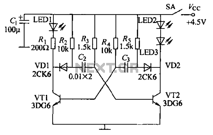
Transistors VT1, VT2, and associated RC components are configured to form a multivibrator. The multivibrator operates with resistors Ra and R4 serving as base bias resistors for VT2 and VT1, respectively. When the switch SA is closed after applying...
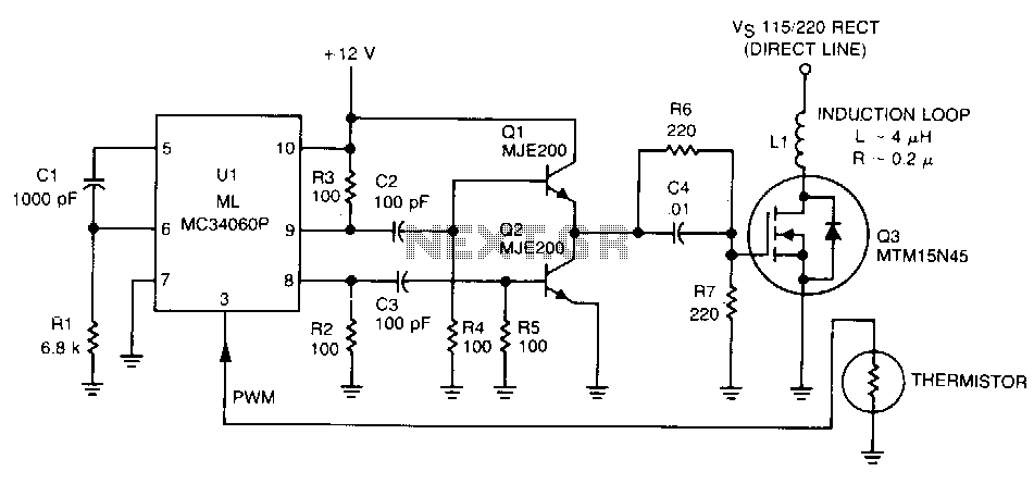
Variable width pulses with fast rise times are generated by the UL and MC34060 operating at 120 kHz, which is the optimal frequency for heating aluminum alloy containers. The pulse width is modulated by monitoring the temperature of the...
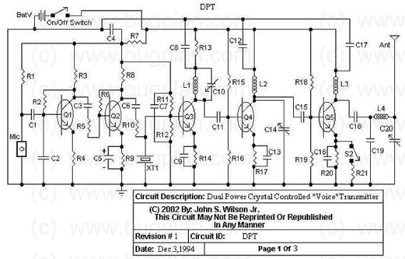
The DPT Transmitter is a dual-powered voice transmitter designed to operate in two modes: a high-power mode for long-range transmission and a low-power mode for extended battery life. It functions at a low power level of 100 mW and...
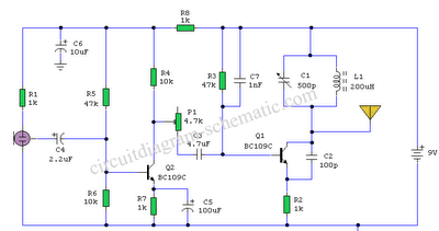
The AM transmitter circuit consists of an audio amplifier and an RF oscillator. The oscillator is constructed around transistor Q1 and its associated components. The tank circuit, which includes inductor L1 and variable capacitor VC1, is tunable from approximately...
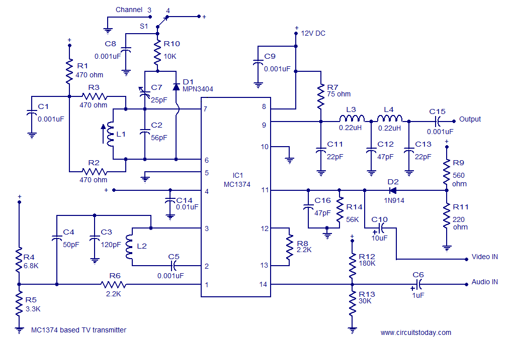
A simple TV transmitter circuit utilizing the TV modulator circuit IC MC1374. It operates with a 12V supply and is capable of broadcasting on channel 3 or 4, employing FM modulation for sound transmission. The TV transmitter circuit based on...
This infrared transmitter is designed for use with an infrared receiver. It operates using either two 1.5V batteries or a 3V lithium battery, allowing for a compact infrared communication system. The infrared transmitter circuit typically consists of an infrared LED,...