
5 Watt audio amplifier
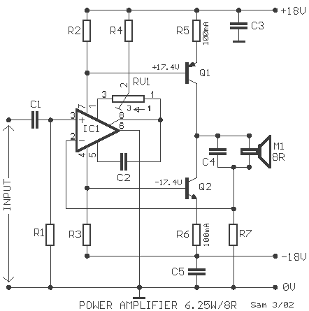
R1 = 10 kΩ, C1 = 470 nF 100V MKT, Q1 = BD242C, R2-3 = 130 Ω, C2 = 22 pF ceramic, Q2 = BD241C, R4 = 68 kΩ, C3-5 = 100 nF 100V MKT, RV1 = 100 kΩ trimmer, R5-6 = 1 Ω 1W, C4 = 220 nF 100V MKT, M1 = 8 Ω >20W Loudspeaker.
The described circuit represents a Class A amplifier utilizing negative current feedback to stabilize the output characteristics and enhance linearity. The configuration allows the amplifier to maintain a consistent load current primarily dictated by the input signal, which is a crucial aspect for audio applications. The feedback loop formed by the voltage across R7 and its connection to the inverting input of the operational amplifier (IC1) ensures that the output remains responsive to variations in the input signal while minimizing distortion.
The gain formula, (Zo + R7) / R7, illustrates how the loudspeaker's impedance directly influences the amplifier's overall gain. The selected values for R7 and the loudspeaker impedance (8Ω) yield a substantial gain of 17, allowing for effective amplification of audio signals.
Quiescent current settings are critical in Class A amplifiers, where the idle state consumes significant power. The design specifies a quiescent current range of 50 to 100 mA, adjustable through R2, R3, R5, and R6. This careful selection of resistors ensures that the transistors operate within their optimal range, promoting efficiency and reducing heat generation.
Transistor matching between Q1 (BD242C) and Q2 (BD241C) is essential to achieve balanced performance and minimize thermal drift. The recommendation to adjust R2 and R3 for bias symmetry further emphasizes the importance of maintaining equal operating conditions for both transistors, enhancing reliability and performance stability.
The output stage of the amplifier is designed to handle an output power of 5W into an 8Ω load while maintaining a remarkably low THD of 0.01%. This level of distortion is indicative of the amplifier's high fidelity, making it suitable for high-quality audio applications. The use of power supply voltages of ±18V provides sufficient headroom for dynamic audio signals, ensuring that the amplifier can deliver peak performance without clipping.
Overall, the circuit is a well-thought-out design that balances performance, efficiency, and audio fidelity, making it a suitable choice for various audio amplification tasks. The amplifier of circuit, use negative current feedback. So, the load current depends mainly from the input signal and no so much from the impedance of loudspeaker. The inductor current of loudspeaker develop above in the R7 a voltage. This voltage is drive to the inverting input of IC1, creating thus negative feedback. Total voltage gain of circuit, it depend from the reason of impedance of loudspeaker H1 [ Zo ], to the price of R7.
In the circuit the gain is (Zo+R7)/R7 that is to say (8+0.5)/0.5=17.. The connection output of IC1 in the ground, is extraordinary, but in this way, the current of base of transistors Q1, Q2 is provided by the lines of supply and no by the IC1. The calm current of is 50 until 100mA, for operation in Class A and is determined by R2, R3, R5, R6. Transistors Q1-Q2, should be matching, so that are not created big current and voltage of deviation. May it will are change the resistors R2, R3, so that we achieve symmetry of bias. With complete drive, the current of emitter the Q1-Q2 is roughly 500mA. The THD is 0.01% for output power, 5W in 8R and voltage supply ± 18V. R1=10Kohm C1=470nF 100V MKT Q1=BD242C R2-3=130ohm C2=22pF ceramic Q2=BD241C R4=68Kohm C3-5=100nF 100V MKT RV1=100Kohm trimmer R5-6=1ohm 1W C4=220nF 100V MKT M1=8ohm >20W Loudspeaker 🔗 External reference
Related Circuits
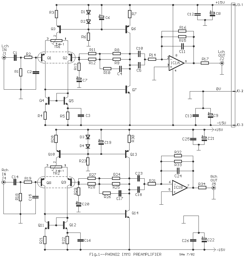
In this circuit exists a second designing proposal of preamplifier RIAA. The first stage uses discernible components and in second exist a opamp. [IC1]. In the negative feedback exist the correction RIAA filters. Certain points need certain discriminators: 1]...
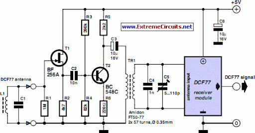
A popular project among microcontroller enthusiasts is to build a radio-controlled clock. Tiny receiver boards are available, featuring a pre-adjusted ferrite. The radio-controlled clock project leverages a microcontroller to receive time signals transmitted from a time signal transmitter, typically operated...
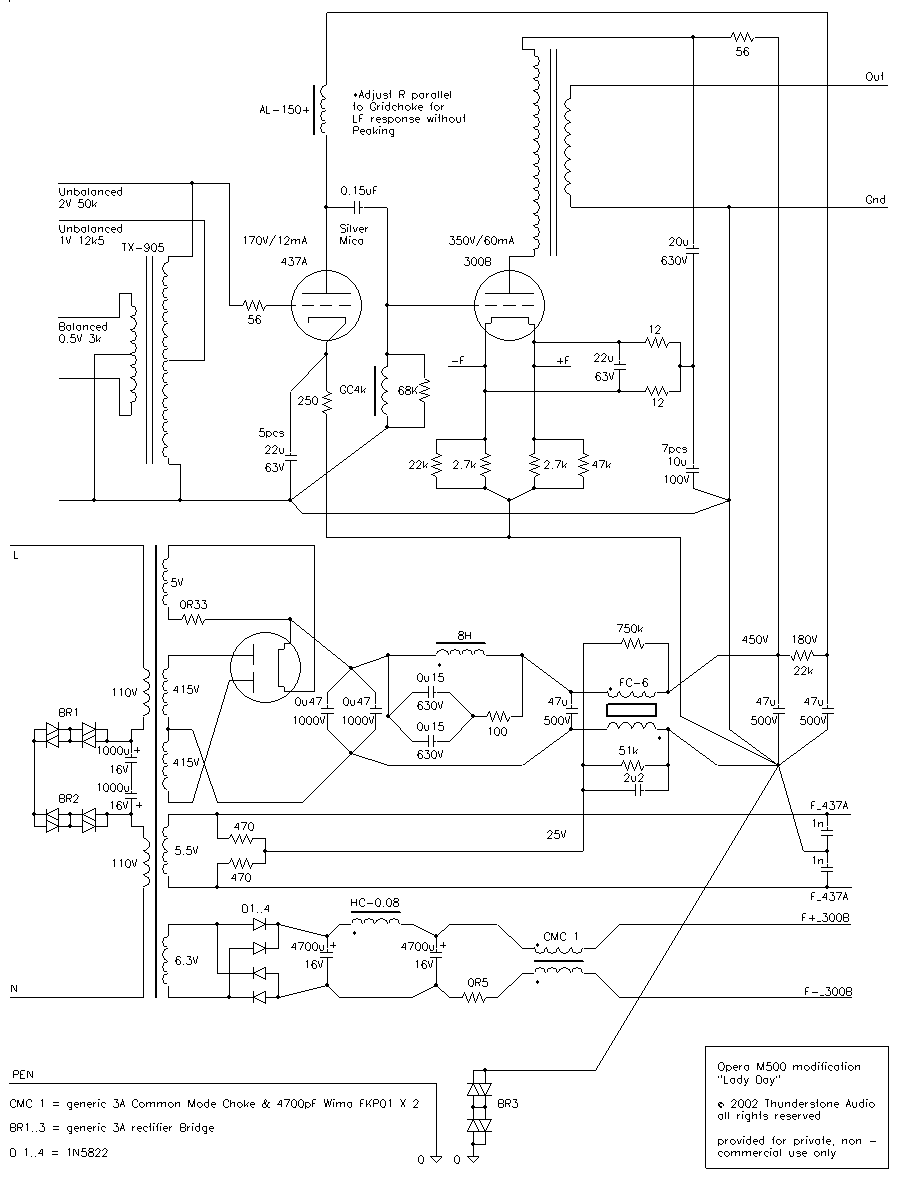
A request for a DIY 300BSE power amplifier schematic is made, with a specification to utilize Lowther PM6 speakers. The 300BSE power amplifier is a well-regarded audio amplification circuit known for its warm sound and high fidelity, particularly suited for...
This project requires expensive hardware, including a microphone and amplifier, along with sophisticated audio analysis on the microcontroller. Even a complete microphone with an amplifier circuit does not yield the desired results, as noted in the product comments. The...
A board design intended for measuring a load cell has been identified with a system accuracy fault traced to the amplifier integrated circuit (IC). The output of the amplifier IC changes when the board is twisted, yielding +80mV when...
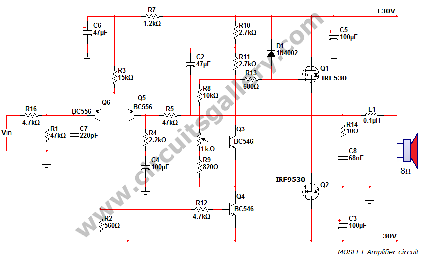
This is a MOSFET transistor-based power amplifier circuit that operates within a voltage range of +35V to -35V. The input voltage is pre-filtered and pre-amplified before being applied to the MOSFET switch. The pre-audio amplifier consists of a differential...