
amplifier Amp measures board twist (unfortunately!)
")
The board design serves to measure a load cell's output voltage, which is influenced by mechanical stress applied to the circuit. The observed variations in the amplifier's output voltage upon twisting the board indicate a potential sensitivity to physical stressors. The load cell is typically composed of a Wheatstone bridge configuration, where the resistance changes due to applied loads, converting mechanical force into an electrical signal.
The amplifier IC is critical in amplifying the small voltage changes from the load cell, but the lack of common mode rejection could result in inaccuracies. This issue can be exacerbated by the physical layout of the components on the board. The twisting of the board introduces mechanical stress, which may affect the amplifier's performance due to the rigid nature of the SOIC package. It is essential to consider the thermal and mechanical properties of the materials used in the circuit design, as these can significantly impact the accuracy of the measurements.
To mitigate these issues, the circuit design should include proper grounding techniques, appropriate placement of decoupling capacitors, and consideration of the layout to minimize thermal gradients. Utilizing a more compliant package for the amplifier or employing techniques such as compliant thermal compounds can help reduce stress on the silicon die.
In summary, the design and testing of the load cell measurement circuit must account for both electrical and mechanical factors. The proposed modifications, including the use of compliant leads and careful attention to component placement, can lead to improved performance and reliability of the load cell measurements. Further testing and validation will be necessary to confirm these adjustments effectively address the accuracy issues observed.A board design that is supposed to measure a loadcell. We have finally tracked a system accuracy fault down to the amp IC. When we twist the board, the amp IC changes its output. I get +80mV when I twist the board from its 4 corners. I`m using the amount of twist that I use to unlock my car with my car key. I get -80mV when I twist the other way. The amount of twist is proportional to the variance in output voltage. To isolate the amp circuit, I have shorted its input and disconnected other circuits from it so that what you see in the diagram is what we`re testing with. If you can, a photo of the board would help us see physical factors that could contribute to the issue.
Are the passives leaded or smt, and what size Where is the circuit located on the board, in the center or near an edge The Photon Apr 23 `13 at 5:20 I`d guess you ARE measuring a load cell - made with copper tracks, although the voltages seem far larger than reasonable. As shown your IC has no common mode restraint on the input circuit (pins 2 & 3, shorted). Look at the datasheet table 8 page 21 and the several pages of related comment preceding it and ensure you are not violating any limits there.
(THey MAY just be putting common sense in a complicated way - hard to be sure without wading through it. My wife says its time to go and buy the Subway 12" special offer, so. ) Russell McMahon Apr 23 `13 at 5:58 Re: ". Good point. I should have shown on the schematic that my shorted inputs are still connected into the 350 ohm loadcell bridge.
So that should take care of this problem. . " Good. Another step forward. In a few more days we may have half the circuit diagram :-). It would be `really wise` to show us the circuit in entirety at least as far as all voltages and currents are concerned. What is the value of AVdd. What is the load cell voltage (AVdd ) and what is the mean DC input voltage (AVdd/2, AVloadcall/2, AV.
) None of this may be of any relevance. All of it might be. Russell McMahon Apr 23 `13 at 7:58 Rebuke accepted, RM. I tried to present the real minimal test circuit but I missed some. I have updated the schematic to include the loadcell even though it is shorted. Berwyn Apr 23 `13 at 22:29 There are known effects like this that need to be taken into account for high precision circuits. Thermal gradients can also have adverse effects, component orientation across or along stress and thermal gradients etc.
Of course we have to do some guessing because we can`t magically know what is in the package. But an educated guess is that the die is either eutectic bonded or glued very rigidly to the bottom of the package cavity. A small SOIC package is very non compliant (i. e. rigid) so the stresses translate directly into the package die cavity floor and then through the die attach into the Si substrate.
Stress can adversely affect Si performance by affecting the electron/hole mobility and Si has known piezo resistance (through similar effects of lattice changes). In fact Intel uses localized stress to increase the performance of PMOS transistors at some process nodes.
In laying out precision circuits in silico it is recommended that sensitive amplifiers in Si not have metal layers over them so that the transistors are not adversely affected. (but here it is a matching issue). to test the hypothesis: I recommend desoldering the amplifier, and then attaching short stubs of PTH (resistor would work) leads to lift the package up off the PCB so the stress doesn`t translate into the package.
Once you`ve fiddled with this and re-fired it up. You should see a change and therefore a verification. USe the new "legs" as compliant members. Or use solder braid if you want to get really carried away. Solutions a DIP version of the same part will have less of an issue because the leads are compliant. In that case using a compliant thermal compound under the package to get heat out might be used. You s 🔗 External reference
Related Circuits
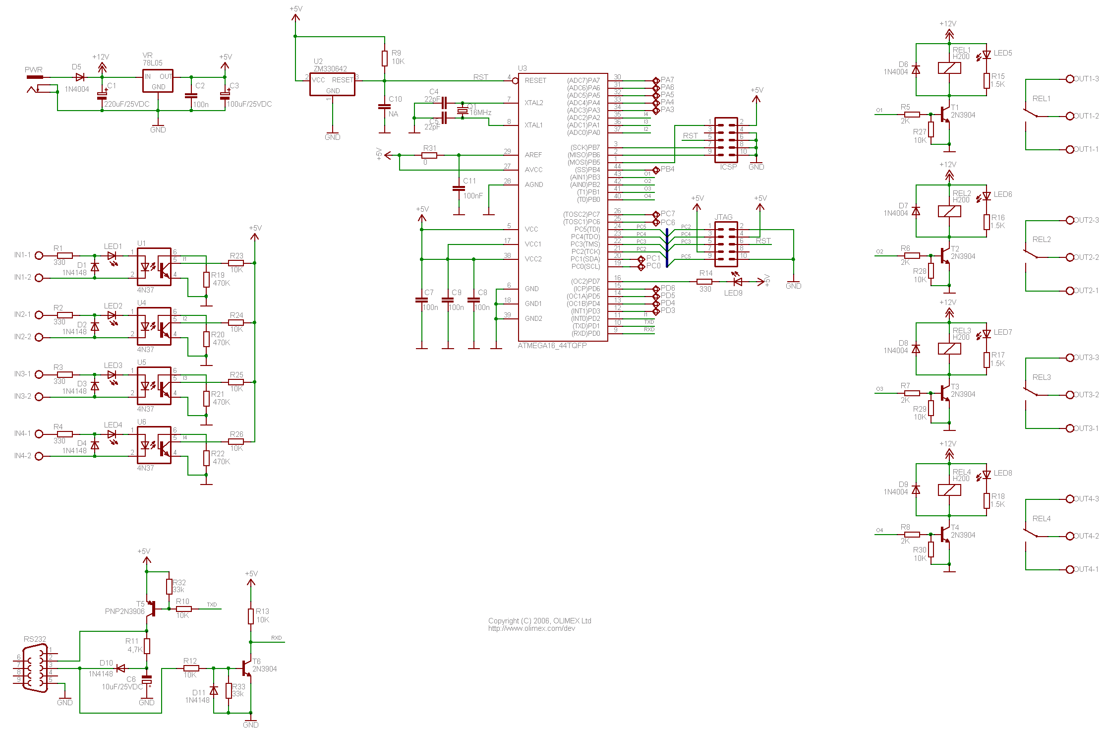
Development board featuring high-power relays, opto-coupled inputs, a power supply circuit, a crystal oscillator circuit, and an RS232 port, along with ICSP and JTAG ports. The JTAG connector utilizes a 5x2 pin configuration for in-circuit programming. This development board is designed...
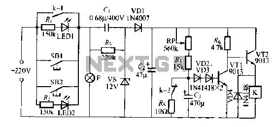
The lamp relay delay circuit is illustrated in Figure 7. Components S131 and SB2 are light buttons mounted in different locations. The lamp can operate with F. LEDs (LED1 and LED2) should be installed in SB1 and SB2 to...
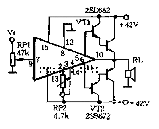
The AP500A amplifier offers numerous advantages, providing unmatched superiority in stereo applications. It can utilize various amplifier configurations, including OTI, CI, rK, BTL, class AB, and super CP. The typical DC amplifier module for the AP500A is illustrated in...
Not so much a real project as a field day for experimenters, this article describes the methods you can use to tailor an amplifier to a specific driver. Much is empirical (i.e. design by experiment, trial and error), and...
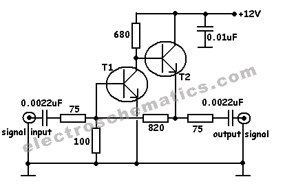
This cable TV amplifier circuit is an RF amplifier designed for quick installation between two coaxial cables. Both the input and output impedances are compatible with 75-ohm cables. The main amplifier is the T1 transistor, while T2 functions as...
.jpg)
The HID ballast circuit consists of a buck stage for regulating lamp current and power, a full-bridge output stage that generates a low-frequency (200Hz) AC square-wave voltage and current to drive the lamp, and an ignition circuit that produces...