
500KW Transmitter Schematic
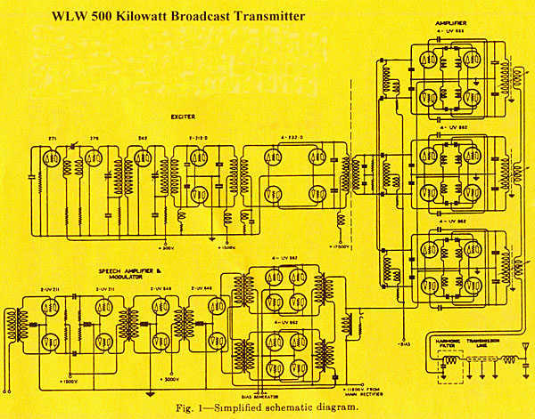
The described transmitter employs a modular architecture to enhance reliability and maintain operational continuity. The final amplifier is segmented into three distinct modules, each housing four RCA type UV-898 vacuum tubes, arranged in a push-pull parallel configuration. This design results in a total of twelve output tubes, which collectively amplify the RF signal.
The series combination of the outputs from the three modules allows for operational redundancy. In the event of a failure in one of the RF modules, the transmitter can continue functioning utilizing the remaining modules. This redundancy is crucial for maintaining service, especially in critical broadcasting applications.
The modular approach not only improves reliability but also facilitates easier maintenance and upgrades. Each module can be serviced or replaced independently without taking the entire transmitter offline. The design reflects a modern trend in transmitter engineering, where solid-state components are increasingly used in a similar modular format, typically featuring 1 kW power modules. These lower power modules are particularly beneficial for applications requiring shallow modulation slopes, ensuring that the transmitter can adapt to various operational demands while maintaining signal integrity.
Overall, the transmitter's design exemplifies advancements in RF amplifier technology, emphasizing the importance of redundancy and modularity in ensuring continuous service in broadcasting applications.The transmitter was designed with redundancy and cutback (reduced power mode) in mind, giving the transmitter more continuity of service. The final amplifier was divided into 3 separate modules, each using four RCA type UV-898 tubes in push-pull parallel making up a total of 12 output tubes.
The outputs of the three modules were combined in series in such a way, that if one of the 3 RF modules failed, the transmitter could continue to operate using the other modules. This idea was a very important step in transmitter design as modern solid-state transmitters are designed entirely in this a modular fashion as is described in my WABC Digital AM Transmitter Page Digital Modulation Section.
Modern transmitter with modular design are composed, typically of 1KW modules with lower power modules used for shallow slopes of modulation. 🔗 External reference
Related Circuits

A 27MHz transmitter circuit schematic utilizing the MC2833 and two FET transistors, MPF6660. This design incorporates a Motorola MC2833 one-chip FM transmitter along with several supporting components. The 27MHz transmitter circuit is designed to operate within the FM radio frequency...
FM Wireless Microphone Schematic. In some applications, using a microphone cable can be quite challenging, necessitating the use of a cordless microphone, commonly referred to as a wireless microphone. This document presents a wireless microphone circuit schematic that utilizes...
A simple USB FM transmitter that can be used to play audio files from an MP3 player or computer on a standard VHF FM radio by connecting it to a USB port. The circuit does not require any coils...

The circuit depicted in Figure 8 is a low-pass filter utilizing an eight-stage switched-capacitor configuration. The cutoff frequency of the circuit can be adjusted, with a clock frequency that can be modified to 1/100 of the original frequency. A...

The circuit incorporates components Q, C, and ZD, which are responsible for the bias and buffer stages. Its primary objective is to ensure stable MOSFET gate operation and provide an offset voltage through a voltage buffer amplifier stage with...

This is a single-chip FM transmitter circuit utilizing the Maxim semiconductors IC MAX2606. The MAX2606 is a compact, high-performance intermediate frequency voltage-controlled oscillator (VCO) specifically designed for wireless communication applications. It features a monolithic construction that ensures low noise...