
50WOTL amplifier circuit
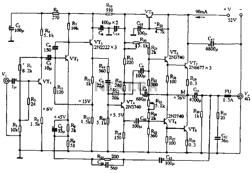
The OTL amplifier circuit is designed for high fidelity and low distortion audio amplification, making it suitable for high-end audio applications. The frequency response range of 10 Hz to 100 kHz allows it to reproduce a wide spectrum of audio frequencies, ensuring that both low and high frequencies are accurately amplified. The low total harmonic distortion (THD) of less than 0.1% indicates that the amplifier can deliver a clean and accurate audio signal, minimizing unwanted artifacts that can affect sound quality.
The circuit's architecture is divided into four distinct stages, each serving a specific function. The input stage is responsible for receiving the audio signal and preparing it for further amplification. The impedance converter stage matches the input impedance to the subsequent stages, ensuring efficient signal transfer. The power output stage amplifies the signal to a level suitable for driving speakers, while the inverter stage serves to further enhance the output signal's characteristics.
The use of local feedback at each stage helps in maintaining stability and preventing oscillations, which can be a common issue in high-gain amplifier designs. By avoiding large DC negative feedback loops, the circuit retains its dynamic range and responsiveness, which is crucial for high-quality audio reproduction.
The choice of a high-value resistor in the emitter circuit of VT2 contributes to the overall stability and performance of the amplifier. This design decision helps to ensure that the operating point remains fixed, even with variations in input signal levels or component tolerances. The coupling capacitor (C3) plays a vital role in blocking DC while allowing AC signals to pass, ensuring that only the desired audio frequencies are amplified.
Finally, the output impedance reduction achieved through the emitter output of VT3 allows for better interaction with the load (speakers), improving the amplifier's overall performance and efficiency. This careful consideration of component values and circuit topology results in a robust OTL amplifier capable of delivering high-quality audio with minimal distortion.Circuit shown in Figure. Higher technical specifications of the circuit, is a very good OTL amplifier circuit. The frequency response of the circuit of 10Hz ~ 100kH, total harmonic distortion <0.1%, which is not much in general (YFL power amplifier see o barrier circuit consists of four parts: the input stage, impedance converter stage, and power output of the inverter stage level. interstage resistance and capacitance coupling units, no large DC negative feedback loop, since each level plus deeper local feedback, so the working point of the circuit is very stable fixed O VTi and peripheral components of the input stage, in order to increase the input impedance of the circuit and stability ,, rTc emitter using a high-value resistor 1_5kfl of O VT2, VT3 composed of direct-coupled amplifier input stage and it is coupled by a capacitor C3 o Rl l-oriented electrical negative feedback stage resistance, to stabilize the operating point of the level oVT3 using emitter output, to reduce the output impedance, easy and inverter stage VT4 match, improve inverter stage VT4 push capability.
Related Circuits

Floating the grid above ground is detrimental for RF performance and arc protection. The connection of the control grid to ground is critical for stability. It is essential to keep the grid connection to ground as wide and short...
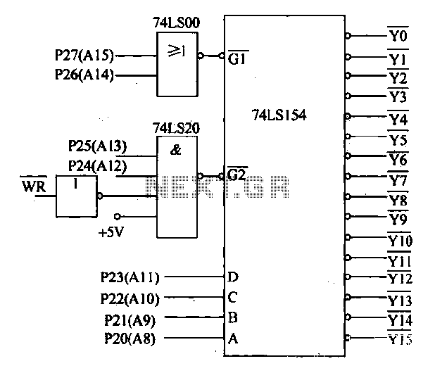
Decoding circuit: To ensure proper functionality of various interfaces, the system must assign IP addresses to all ports. Based on the number of system interfaces, it utilizes the 74LS154 decoder, which can translate up to 16 addresses. The interface...
High Power Siren Circuit. This article discusses a robust siren circuit suitable for various applications. A complementary transistor pair (BC557 & BC337) is configured as an oscillator to directly drive the speaker. Transistor Q1 (BC557) is utilized to ensure...
This circuit is a conventional Pierce type oscillator that utilizes a JFET. It employs fundamental mode crystals and demonstrates good performance and reliability when a low noise JFET is used. The feedback is regulated by the capacitance C1, which...
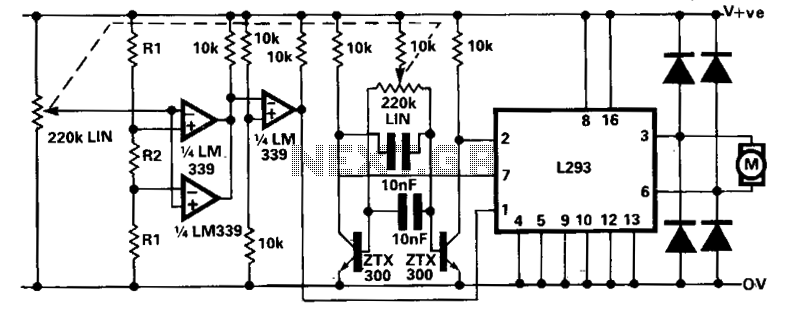
A limitation of the bi-directional proportional motor control circuit is that when the potentiometer is in its center position, the motor does not stop but continues to creep. This occurs due to the challenge of precisely adjusting the potentiometer...
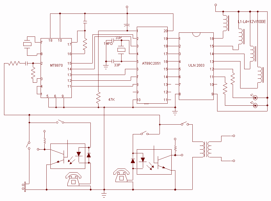
This project is used as an electronic private exchange. It has two telephones, which have the intercom facility, and they can be connected to the telephone line. All the functions are controlled by the 8-bit microcontroller AT89C2051 which has...
Warning: include(partials/cookie-banner.php): Failed to open stream: Permission denied in /var/www/html/nextgr/view-circuit.php on line 713
Warning: include(): Failed opening 'partials/cookie-banner.php' for inclusion (include_path='.:/usr/share/php') in /var/www/html/nextgr/view-circuit.php on line 713