
555 Timer as an Astable Multivibrator
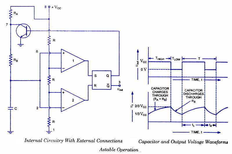
The astable multivibrator circuit configuration using the 555 timer integrates two resistors (RA and RB) and a capacitor (C) to establish a continuous oscillation between high and low output states. The arrangement of these components determines the frequency and duty cycle of the generated square wave signal. The resistors and capacitor form an RC timing network, where the charge and discharge cycles of the capacitor dictate the timing intervals. The output waveform can be analyzed using an oscilloscope to visualize the transitions between the high and low states, confirming the functionality of the circuit.
The choice of resistor values and the capacitor's capacitance will directly influence the oscillation frequency. The equations governing the timing intervals allow for precise calculations to achieve desired output characteristics. It is essential to consider the tolerances of the components used, as variations can affect the stability of the output waveform. Additionally, the implementation of a diode across RB enhances performance by ensuring a more symmetrical waveform, which is critical in applications requiring accurate timing signals.
In practical applications, the astable multivibrator can be utilized in various circuits, including clock pulses for digital circuits, tone generators, and flashing LED indicators. The versatility of the 555 timer, combined with the simplicity of the astable configuration, makes it an invaluable component in electronic design. When deploying the 7555 CMOS variant, designers benefit from improved efficiency and reduced noise, further enhancing the reliability of the circuit in sensitive applications.An astable multivibrator, often called a free-running multivibrator, is a rectan gular-wave generating cir cuit. Unlike the monostable multivibrator, this circuit does not require any ex ternal trigger to change the state of the output, hence the name free-running.
Before going to make the circuit, make sure your 555 IC is working. For that go through the article: How to test a 555 IC for working An astable multivibrator can be produced by adding resistors and a capacitor to the basic timer IC, as illustrated in figure. The timing during which the output is either high or low is determined by the externally connected two resistors and a capacitor.
The details of the astable multivibrator circuit are given below. Pin 1 is grounded; pins 4 and 8 are shorted and then tied to supply +Vcc, output (VOUT is taken form pin 3; pin 2 and 6 are shorted and the connected to ground through capacitor C, pin 7 is connected to supply + VCC through a resistor RA; and between pin 6 and 7 a resistor RB is connected. At pin 5 either a bypass capacitor of 0. 01 F is connected or modulation input is applied. In figure, when Q is low or output VOUT is high, the discharging transistor is cut- off and the capacitor C begins charging toward VCC through resistances RA and RB.
Because of this, the charging time constant is (RA + RB) C. Eventually, the threshold voltage exceeds +2/3 VCC, the comparator 1 has a high output and triggers the flip-flop so that its Q is high and the timer output is low. With Q high, the discharge transistor saturates and pin 7 grounds so that the capacitor C discharges through resistance RB with a discharging time constant RB C.
With the discharging of capacitor, trigger voltage at inverting input of comparator 2 decreases. When it drops below 1/3VCC, the output of comparator 2 goeshigh and this reset the flip-flop so that Q is low and the timer output is high. This proves the auto-transition in output from low to high and then to low as, illustrated in fig ures.
Thus the cycle repeats. The time during which the capacitor C charges from 1/3 VCC to 2/3 VCC is equal to the time the output is high and is given astc or THIGH = 0. 693 (RA + RB) C, which is proved below. td or TL0W = 0. 693 RB C where RB is in ohms and C is in farads The above equation is worked out as follows: Voltage across the capacitor at any instant during discharging period is given as Overall period of oscillations, T = THIGH + TLOW = 0.
693 (RA+ 2RB) C, The frequency of oscillations being the reciprocal of the overall period of oscillations T is given as From the above equation it is obvious that square wave (50 % duty cycle) output can not be obtained unless RA is made zero. However, there is a danger in shorting resistance RA to zero. With RA = 0 ohm, terminal 7 is directly connected to + VCC. During the discharging of capacitor through RB and transistor, an extra current will be supplied to the transistor from VCC through a short between pin 7 and +VCC.
It may damage the transistor and hence the timer. However, a symmetrical square wave can be obtained if a diode is connected across resistor RB, as illustrated in dotted lines in figure. The capacitor C charges through RA and diode D to approximately + 2/3VCC and discharges through resistor RB and terminal 7 (transistor) until the capacitor voltage drops to 1/3 VCC.
Then the cycle is repeated. To obtain a square wave output, RA must be a combination of a fixed resistor R and a pot, so that the pot can be adjusted to give the exact square wave. Although the timer 555 has been used in a wide variety of often unique applications it is very hard on its power supply lines, requiring quite a bit of current, and injecting many noise transients.
This noise will often be coupled into adjacent ICs falsely triggering them. The 7555 is a CMOS version of the 555. Its quiescent current requirements are considerably lower than that of 555, and the 7555 does not contaminate the power supply lines. It is pin compatible with the 555. So this CMOS version of the 555 should be the first choice when a 555 timer IC is to be used. 🔗 External reference
Related Circuits
The 555 timer integrates both analog and digital functions within a scaled integrated device. Typically manufactured using a bipolar process, it is designated as the 555 timer, while the CMOS version is referred to as the 7555. In addition...
This can be a thin strand of wire, like one of the copper "hairs" from a section of lamp cord, which is wired to the altimeter by terminals somewhere on the rocket body and anchored to the launch stand...
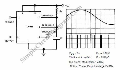
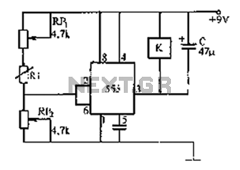
A simple pulse modulator circuit can be constructed using a 555 integrated circuit (IC). The 555 chip features a special modulator input located at pin 5. Below is the schematic diagram of the circuit. The pulse modulator circuit utilizing the...
The primary concept is to rotate the motor slightly every 15 seconds. A monofilament line conveys the motion to the ornament, which is wound by the motor and gradually unwinds as the ornament turns. The charging circuit includes a...
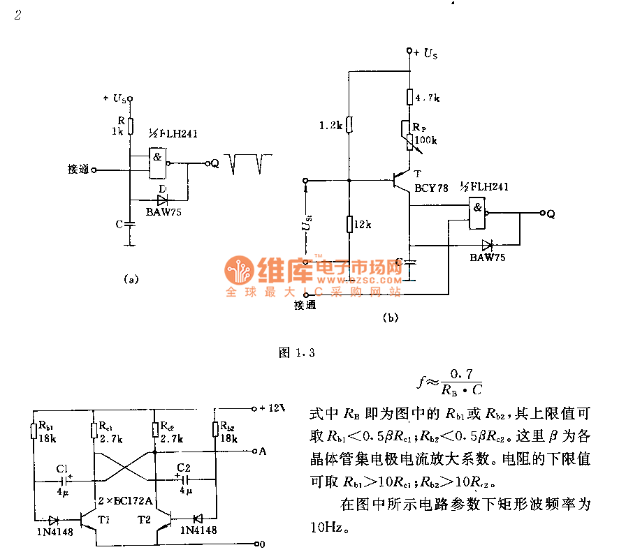
The circuit consists of two components whose parameters and models are designed to simultaneously generate a rectangular wave with a duty cycle of 1:1. The frequency is defined by the equation f = 0.7/(RB * C), where RB refers...

An astable multivibrator can be designed using a 555 timer IC, operational amplifiers, or transistors. The 555 timer IC provides accurate time delays ranging from milliseconds to hours, with the frequency of oscillation adjustable through simple modifications. This is...
Warning: include(partials/cookie-banner.php): Failed to open stream: Permission denied in /var/www/html/nextgr/view-circuit.php on line 713
Warning: include(): Failed opening 'partials/cookie-banner.php' for inclusion (include_path='.:/usr/share/php') in /var/www/html/nextgr/view-circuit.php on line 713