
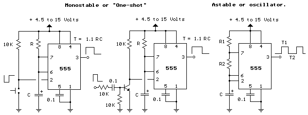
555 Timer Frequency and Duty Cycle Calculator
Pin 1 (Ground) - This pin serves as the most negative supply potential of the device, typically connected to circuit common when powered by positive supply voltages.
Pin 2 (Trigger) - This input pin initiates the output transition to a high state, starting the timing cycle. Triggering occurs when the voltage at this pin drops from above 2/3 of the supply voltage to below 1/3. For example, with a 12-volt supply, the trigger voltage should start above 8 volts and drop below 4 volts to commence the timing cycle. The triggering action is level-sensitive, and the trigger voltage may change slowly. To prevent retriggering, the trigger voltage must exceed 1/3 of the supply before the end of the timing cycle in monostable mode. The trigger input current is approximately 0.5 microamps.
Pin 3 (Output) - This output pin transitions to a high level of approximately 1.7 volts less than the supply voltage at the start of the timing cycle and returns to a low level near 0 volts at the end of the cycle. The maximum output current, whether in low or high state, is about 200 mA.
Pin 4 (Reset) - A low logic level on this pin resets the timer and sets the output to a low state. It is typically connected to the positive supply line when not in use.
Pin 5 (Control) - This pin enables modification of the triggering and threshold voltages by applying an external voltage. In astable or oscillating modes, this input can be used to alter or frequency modulate the output. If not utilized, it is advisable to connect a small capacitor from pin 5 to ground to mitigate potential false triggering due to noise.
Pin 6 (Threshold) - This pin is responsible for resetting the latch and causing the output to transition to a low state. Resetting occurs when the voltage at this pin rises from below 1/3 of the supply to above 2/3. The action is level-sensitive and can change slowly, similar to the trigger voltage.
Pin 8 (V +) - This pin serves as the positive supply voltage terminal for the 555 timer IC, with an operating voltage range of +4.5 volts (minimum) to +16 volts (maximum). The pin connections for the 556, which is a dual 555 timer (two timers in one package), are detailed in the accompanying table. For instance, the outputs for the two timers of the 556 are located on pins 5 and 9, corresponding to the output pin 3 of the 555.
The 555 timer is a versatile device used in various applications, including timers, pulse generation, and oscillators. By adjusting the values of R1, R2, and C, the time intervals and frequency can be tailored to meet specific requirements. The circuit's behavior can be further analyzed by employing simulation software or breadboarding the design to observe real-time performance and adjust component values accordingly.Enter values for R1, R2, and C and press the calculate button to solve for positive time interval (T1) and negative time interval (T2). For example, a 10K resistor (R1) and 100K (R2) and 0. 1 uF capacitor will produce output time intervals of 7. 62 mS positive (T1) and 6. 93 mS negative (T2). The frequency will be about 70 Hz. R1 should be greater th an 1K and C should be greater than. 0005 uF. Scroll down page for basic 555 information (pinout and two basic circuits). Pin 1 (Ground) - The ground (or common) pin is the most-negative supply potential of the device, which is normally connected to circuit common when operated from positive supply voltages. Pin 2 (Trigger) - This pin is the input which causes the output to go high and beginthe timing cycle.
Triggering occurs when the trigger input movesfrom a voltage above 2/3 of the supply voltage to a voltage below1/3 of the supply. For example using a 12 volt supply, the triggerinput voltage must start from above 8 volts and move down to avoltage below 4 volts to begin the timing cycle.
The action islevel sensitive and the trigger voltage may move very slowly. Toavoid retriggering, the trigger voltage must return to a voltageabove 1/3 of the supply before the end of the timing cycle in themonostable mode. Trigger input current is about 0. 5 microamps. Pin 3 (Output) - The output pin of the 555 moves to a high level of 1. 7 volts less than the supply voltage when the timing cycle begins. The output returns to a low level near 0 at the end of the cycle. Maximum current from the output at either low or high levels is approximately 200 mA. Pin 4 (Reset): - A low logic level on this pin resets the timer and returns the output to a low state.
It is normally connected to the + supply line if not used. Pin 5 (Control) - This pin allows changing the triggering and threshold voltages by applying an external voltage. When the timer is operating in the a stable or oscillating mode, this input could be used to alter or frequency modulate the output.
If not in use, it is recommended installing a small capacitor from pin 5 to ground to avoid possible false or erratic triggering from noise effects. Pin 6 (Threshold) - Pin 6 is used to reset the latch and cause the output to go low. Reset occurs when the voltage on this pin moves from a voltage below 1/3 of the supply to a voltage above 2/3 of the supply.
The action is level sensitive and can move slowly similar to the trigger voltage. Pin 8 (V +) - This is the positive supply voltage terminal of the 555 timer IC. Supply-voltage operating range is +4. 5 volts (minimum) to +16volts (maximum). The pin connections for the 556 which is a dual 555 timer (2 in one package) areshown in table below. For example, the two outputs for the two timers of the 556 areon pins 5 and 9 which correspond to the output pin 3 of the 555.
🔗 External reference
Related Circuits
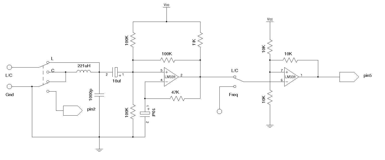
An LC meter is being constructed due to the absence of a multimeter capable of measuring inductance. Although the available multimeters can measure capacitance, they lack accuracy for small capacitance values in the range of several picofarads (pF). While...

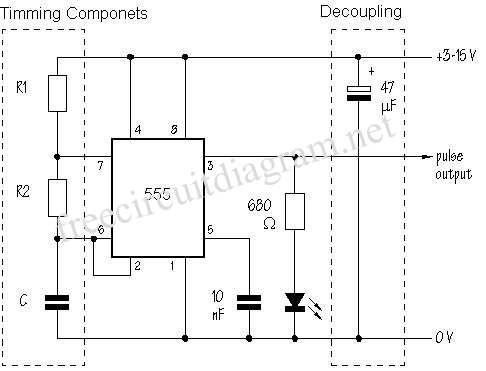
A simple Sump Pump Control Circuit using NE555. The described circuit utilizes the NE555 timer integrated circuit (IC) to create a control system for a sump pump. The NE555 can be configured in various modes, but for this application, it...
The SE555/NE555 timer was first introduced by the Signetics Corporation around 1971. Pin connections and functions are as follows: Pin 1 (Ground) - This pin serves as the ground or common pin, representing the most negative supply potential of...
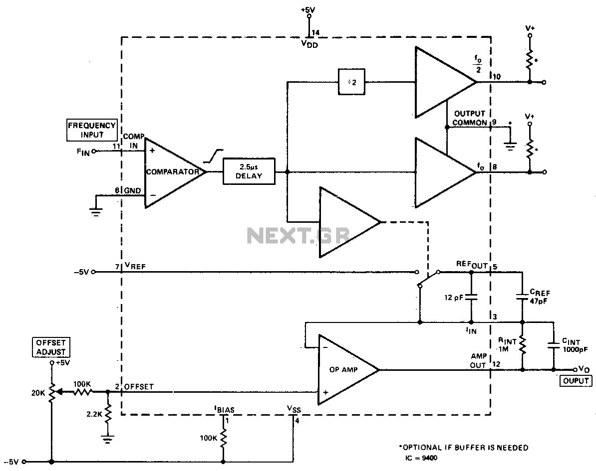
The converter produces an output voltage that is linearly proportional to the input frequency waveform. Each zero crossing at the comparator's input results in a specific amount of charge being dispensed into the op-amp's summing junction. This charge subsequently...
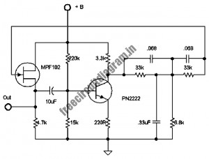
The following circuit illustrates a stable 60 Hz frequency signal generator circuit diagram. Features include a 0.068 µF capacitor incorporated within a feedback loop, allowing for DC-to-AC conversion. This circuit is designed to generate a stable 60 Hz sine wave...

The Servo Timer II was primarily designed for parachute deployment on water rockets but can be used for other applications. The timer controls a single RC servo motor that can open a latch on a parachute door. Once triggered,...