
5V / 2A isolated switching power supply circuit diagram
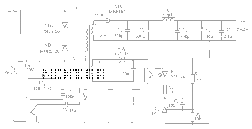
The circuit described is a robust power supply regulation system designed to maintain stable output voltage despite input fluctuations. The input filter capacitor C1 plays a crucial role in smoothing out incoming voltage variations, thus protecting downstream components from transients. The primary clamp formed by VDz and VD1 ensures that any overvoltage conditions are managed effectively, preventing damage to sensitive components.
The use of the TOP414GC-S integrated circuit as a control element highlights the circuit's focus on high efficiency and reliability. By placing this component in parallel with C10, the design mitigates the potential for high-frequency noise, which is critical in maintaining the integrity of the control signals. The output rectification is handled by VD2, ensuring that the alternating current (AC) is converted to direct current (DC) efficiently.
The output filter, consisting of capacitors C3, C4, and inductors L, along with additional capacitors C5 and C6, is designed to further smooth the output, reducing ripple and noise. The incorporation of C9 as a noise cancellation capacitor enhances the stability of the output signal, making it suitable for sensitive applications.
The TL431 shunt regulator serves as an external error amplifier, providing precise voltage regulation. The feedback mechanism, facilitated by resistors R3 and R4, allows for real-time monitoring and adjustment of the output voltage, ensuring that it remains within specified limits. The optocoupler PC817A is employed for electrical isolation between the control circuit and the power circuit, enhancing safety and reliability.
Overall, this circuit exemplifies a well-thought-out design that prioritizes stability, efficiency, and protection against electrical noise and fluctuations, making it suitable for various applications in power electronics.Circuit is shown. C1 is the input filter capacitor. VDz VD1 composition and primary clamp .png">protection circuit . The control terminal of the resistor R1, C2 is a bypass capacitor. TOP414GC-S parallel between the end of the C10 is to prevent high-frequency interference appears on the control side sometimes cause power outages trigger circuit malfunction. VD2 output rectifier diode, output filter C3, C4, L, C5 and C6 constituted, C9 as an output capacitor noise cancellation.
External error amplifier by a TL431 shunt regulator composition. When the output voltage fluctuates, by R3, R4 after the voltage obtained by dividing the sample voltage, the TL431 with a reference voltage, and generates an external control signal, and then to change TOP414G control terminal current through optocoupler PC817A, thereby regulating the duty than make Uo stabilize. Control loop gain is set by R2. After the feedback winding voltage VD3, after C7 rectifier to PC817A the infrared receiver power supply.
Related Circuits

Designing a power supply that meets the requirements of Power over Ethernet (PoE) and Voice over Internet Protocol (VoIP) applications can be complex. The low-component-count power supply illustrated in the figure complies with these specifications without requiring intricate circuitry....
The ultrasonic cleaning machine functions as a humidifier and operates on a simple circuit primarily consisting of an ultrasonic oscillator. It generates ultrasonic frequency signals, typically within the range of 20-40 kHz, using a transistor. These signals are transmitted...
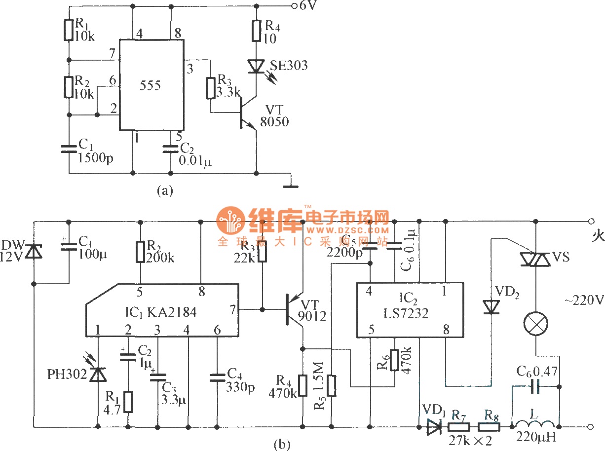
This is an infrared emission circuit diagram. The NE555 circuit generates a 40 kHz pulse, which is sent by the infrared emission control SE303 after being amplified by VT. The remote receiver and infrared dimming circuit are composed of...
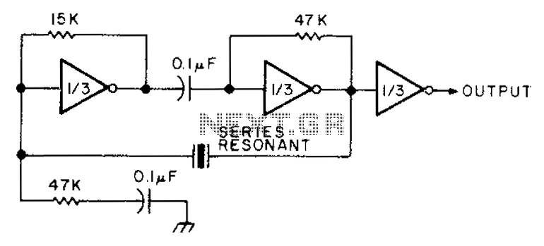
The circuit diagram illustrates the connection of all three components of the series resonant crystal and triple CD4049 inverter. The supply voltage range is between 3 to 15 volts, making it suitable for various applications. This design is compact...
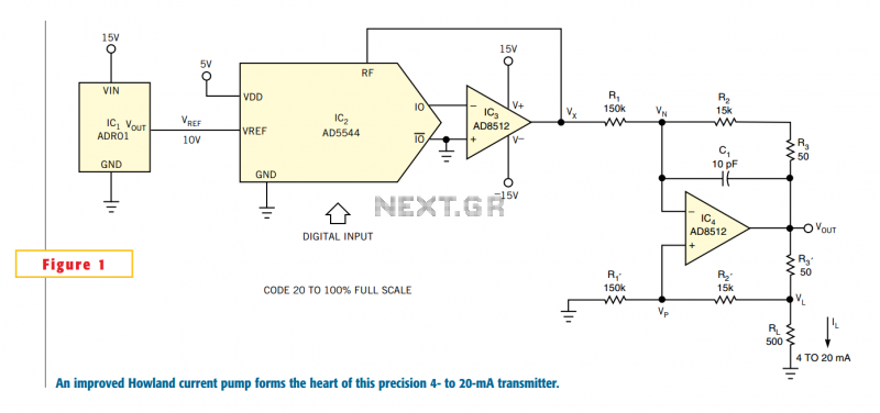
One of the key challenges in the design of 4- to 20-mA current transmitters is the voltage-to-current conversion stage. Conventional transmitters use multiple op amps and transistors to perform the conversion function. These approaches have been around for a...
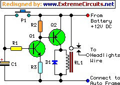
This device is a simple timer that keeps the headlights of a vehicle on for approximately 1 minute and 30 seconds, allowing access to dark areas without the need to manually switch off the lights. Activating switch P1 initiates...
Warning: include(partials/cookie-banner.php): Failed to open stream: Permission denied in /var/www/html/nextgr/view-circuit.php on line 713
Warning: include(): Failed opening 'partials/cookie-banner.php' for inclusion (include_path='.:/usr/share/php') in /var/www/html/nextgr/view-circuit.php on line 713