
5v regulator circuit using lm105

A robust electronic schematic can be derived from the described circuit, which involves a single diffused, wide base transistor like the 2N3740, known for its stability and reliability under various operating conditions. The circuit's design incorporates a pass transistor, which may be a 2N2905 for lower dissipation applications. The careful selection of R1 and R2 resistors is crucial for setting the output voltage, with a target feedback voltage of 1.8V to the LM105’s Pin 6. The combination of these resistors should ideally total around 2K to minimize thermal drift, allowing for some tolerance in their values without compromising performance.
The output capacitor, C2, plays a critical role in maintaining circuit stability by mitigating oscillations within the feedback loop that includes the external booster transistor, Q1. This configuration is vital for ensuring the smooth operation of the LM105 output transistor. Capacitor C1 serves to enhance the stability of the internal regulator circuitry, accommodating varying load conditions effectively. The optional capacitor C3 may be omitted if the physical layout of the circuit is optimized with short lead lengths between the regulator and the rectifier output filter, further enhancing performance and reliability. Overall, this schematic design emphasizes stability, thermal management, and cost-effectiveness, making it suitable for various applications in electronic systems.A single diffused, wide base transistor like the 2N3740 is recommended because it causes fewer oscillation problems than double diffused, planar devices. In addition, it seems to be less prone to failure under overload conditions; and low cost devices are available in power packages like the TO-66 or even TO-3.
When the maximum dissipation in the pass transistor is less than about 0. 5W, a 2N2905 may be used as a pass transistor. However, it is generally necessary to carefully observe thermal deratings and provide some sort of heat sink. In this circuit the output voltage is determined by R1 and R2. The resistor values are selected based on a feedback voltage of 1. 8V to Pin 6 of the LM105. To keep thermal drift of the output voltage within specifications, the parallel combination of R1 and R2 should be approximately 2K.
However, this resistance is not critical. Here is a schematic drawing: Variations of ±30% will not cause an appreciable degradation of temperature drift. The 1 µF output capacitor, C2, is required to suppress oscillations in the feedback loop involving the external booster transistor, Q1, and the output transistor of the LM105.
C1 compensates the internal regulator circuitry to make the stability independent for all loading conditions. C3 is not normally required if the lead length between the regulator and the output filter of the rectifier is short.
🔗 External reference
Related Circuits
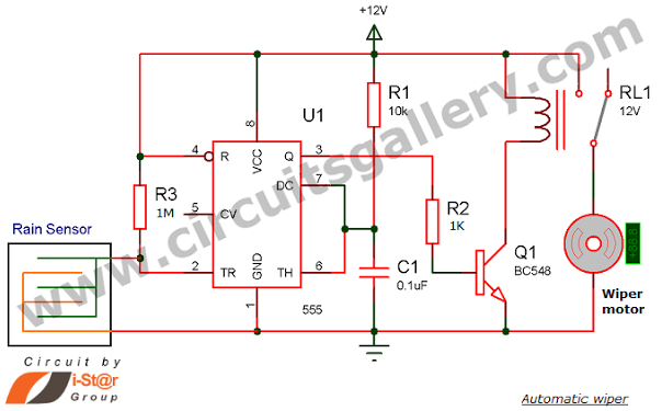
Have you seen Audi, Lexus, or Ford rain-sensing wipers and wondered how they operate in these vehicles? They are controlled by sensors located at the center of the windscreen, which detect raindrops and activate the wiper motor. The functioning...

Have an old hard drive that no longer works? As long as it still spins up chances are you could build a clock out of your old hard drive! You will need some electronic knowledge, some common electronic components...
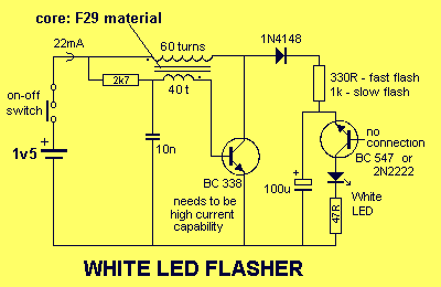
This circuit is very similar to a Joule Thief, but it utilizes two transistors, does not include a transformer core, and employs only one inductor. The described circuit operates on principles akin to those of a Joule Thief, which is...
This simple circuit can be used to charge a pair of AA or AAA-sized cells using solar energy. It has been utilized to maintain the operation of devices such as a Palm Pilot and a Walkman radio continuously. This...
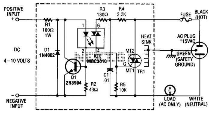
Rl limits input current while Ql acts as a current sink to protect IC1. D1 serves as a polarity protector. IC1 provides a triac output to trigger the main triac, TR1. The circuit consists of several key components that...
This radio modem is widely used for amateur radio packet applications. It is powered by the data and control lines, eliminating the need for additional power sources. The radio modem operates by facilitating packet data communication over amateur radio frequencies....