
Battery Tesla Switch 720 Watt Mosfet Circuits

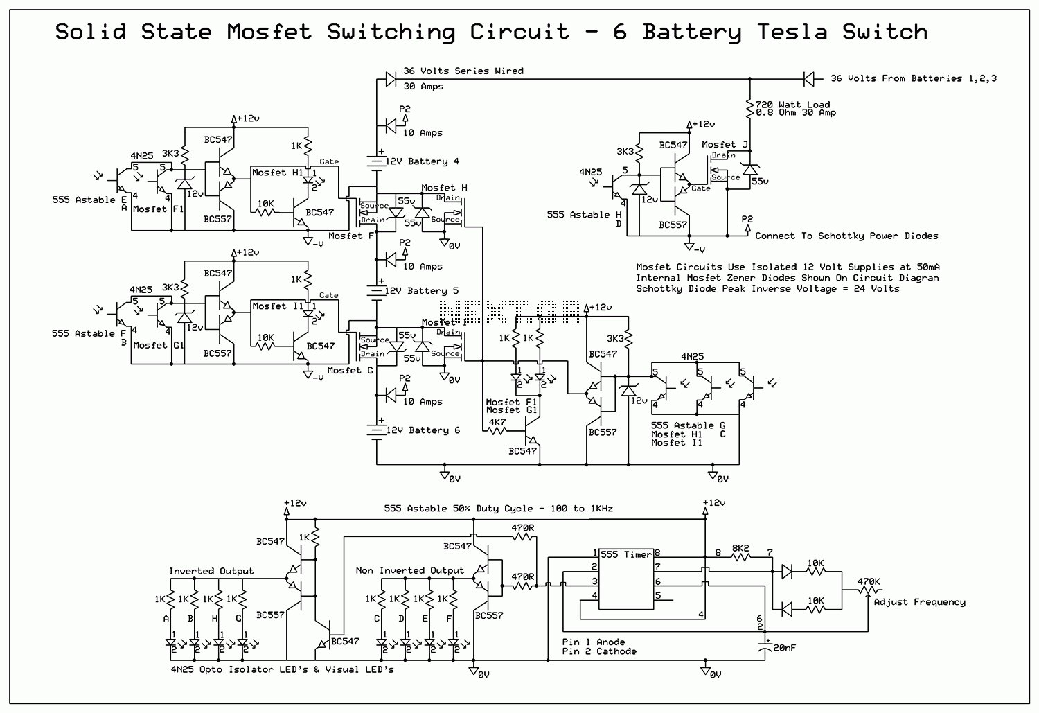
The MOSFET drive circuits utilize isolated 12-volt regulated supplies capable of delivering 50 mA. While ready-built DC-DC converters are available, custom designs can be created for enhanced control. The gates of N-type MOSFETs are driven between 0 volts and +12 volts using transistor pairs in a push-pull configuration. Although logic MOSFETs do not provide advantages in this circuit, they can be used if the gate voltage remains within specified limits. Multiple N-type MOSFETs can be paralleled to decrease circuit resistance, and the push-pull technique allows for rapid charging and discharging of the MOSFET gate capacitance. Heatsinks must be sized according to the continuous current they will handle; the schematic indicates 30 Amps and 10 Amps for the diodes, which can guide the placement of additional parallel MOSFETs. Reducing circuit resistance is crucial, as all components continuously switch and operate at 50% duty cycle, allowing a 30 Amp diode to function at only half its rated capacity. The circuit theoretically can deliver 60 Amps of current to the load, yielding a maximum power output of 1440 watts. Higher voltage Tesla switches should be avoided due to the increased difficulty in sourcing suitable components and elevated costs. This circuit may also be adapted to create switched capacitor charging circuits, functioning similarly to the Tesla switch.
The opto-isolator used in the circuit diagram is the 4N25, which operates as a standard NPN transistor controlled by an internal LED. Resistor values on the 4N25 collector range from 2.2k to 3.3k, while the internal LED requires either a 1k or 470Ω resistor, selected based on the switching frequency. The base of the phototransistor remains unconnected. Despite being a slower device, the 4N25 has been tested to operate effectively between 100 Hz to 1 kHz, eliminating the necessity for a Schmitt trigger opto-coupler. Several opto-isolator transistors are connected in parallel to ensure that no MOSFETs inadvertently turn on at incorrect times. The switching delay, managed by the transistors, lasts approximately 1 microsecond. The transistors employed are NPN BC547 and PNP BC557. Schottky power diodes, such as the SD51, are utilized, and all MOSFETs are N-type with a drain-to-source current rating exceeding 50 Amps and a maximum voltage rating of 55 volts. Integrated Zener diodes in the MOSFETs do not disrupt circuit functionality. Some MOSFETs, designated A, B, F, and G, are oriented backward within the circuit and are driven similarly to the other N-type MOSFETs. When fully activated with a +12V gate-to-source voltage, the MOSFET experiences minimal voltage drop and functions as a switch. When the gate is shorted to the source terminal, the MOSFET ceases conduction, halting current flow. The source and drain terminals of the MOSFETs have been reversed to prevent interference from the internal diode with circuit operation. In this unique configuration, the MOSFETs operate effectively within the Tesla switch circuit, a scenario typically avoided in standard switching circuits due to potential shorting by the body diode. No reverse voltage is observed across the drain and source in the series battery configuration, ensuring current flows solely through the MOSFET channel when the gate is energized. All MOSFETs are rated for 55 volts drain-to-source. A series of 12-volt Zener diodes regulate the base supply voltages in the push-pull circuit. The MOSFET gate drive supply voltages can be clamped using Zener diodes, transistors, or 10-watt resistors. The total circuit consumes approximately 5 watts of power, even when utilizing clamped switched isolated supplies. Any power consumed by the circuit is sourced from the free energy circuit.The circuit uses a total of six, 12 volt lead acid batteries to power the load. 3 batteries are wired in series to create 36 volts. The total discharge current is 30 Amps. 3 batteries are wired in parallel to create 12 volts The total charge current is 10 Amps per battery. 20 Amps are lost to the environment as heat or work done by the load. This is the amount of energy that the environment needs to replace to keep the tesla switch running. A switching circuit is used to set the frequency by which the batteries are changed from series to parallel.
When the switching frequency is high enough, the battery voltage should begin to increase under load. The copper wiring must be constructed from hundreds of thin copper strands, whilst keeping the circuit resistance to an absolute minimum.
All of the connectors should be high quality copper or silver. The output voltage across the load will be approximately 24 volts, & this will have to be regulated in someway using the 555 switching circuit. The capacity of the batteries should be upwards of 40 amps, a small car battery is suitable. The batteries need to deliver 30 Amps through the load, while only getting 10 Amps charging. All of the batteries should have equal capacity & be in good condition.
The mosfet drive circuits use isolated 12 volt regulated supplies which can deliver 50 mA. Dc to dc converters are available ready built, but you can make your own if you need more control over the circuit. The n type mosfet gates are driven between 0 volts & + 12 volts using transistor pairs, in the push pull fashion.
Logic mosfets do not offer any advantage in this circuit, but they can be used if the gate voltage is held within its maximum swing. You can place many n type mosfets in parallel to reduce the circuit resistance. The push pull technique enables very fast charging & discharging of the mosfet gate capacitance, so paralleling mosfets is not a problem.
The heatsinks you use on the components should reflect the amount of continuous current they will carry. On the diagram it shows 30 Amps & 10 Amps for the diodes, which might give you some idea where to place more mosfets in parallel.
Reducing the circuit resistance is a real priority. Since all of the circuit components are constantly switching & are only being used 50 % of the time, this means that a 30 amp diode is only working at 50 % of its rated capacity. Twice the amount of power output is actually available, but only if the circuit resistance can be reduced to less than 0.1 Ohm.
The circuit is capable of delivering 60 amps of current through the load in theory & delivering 1440 watts of power at the maximum. You should avoid making higher voltage tesla switches as it becomes difficult to get hold of suitable components & the cost rises.
You may be able to use this circuit to build switched capacitor charging circuits, which work in the same way as the tesla switch. The opto isolator used in the circut diagram is the 4N25. It is essentially a normal npn transistor, which is controlled entirely using an internal LED. The resistor values on the 4N25 collector are between 2k2 to 3k3. The internal LED requires a 1K or 470R, however this must be chosen depending upon the switching frequency.
The base of the photo transistor is left unconnected. Even though the 4N25 is a slow device, it has been tested to function properly between 100 to 1Kz. There is no need to use a schmitt trigger opto coupler device. A number of opto isolator transistors have been placed in parallel. This is to make absolutely sure that none of the mosfets can turn on at the wrong time. There is a very short time delay between switches, which is controlled entirely by the transistors themselves. The switching delay is automatically controlled & lasts 1 micro second. The transistors used are : npn BC547 & pnp BC557. The schottky power diodes are stud type, such as SD51. The mosfets are all n-type with 50 Amp + drain to source current rating, very low on resistance with 55 volt working voltage.
The mosfets have integrated zener diodes which do not interfere with the circuit operation. Mosfets A,B,F,G are placed backwards in the circuit & are driven in exactly the same way as the other n type mosfets. When the mosfet is turned fully on, +12v gate to source, there is very little voltage drop across the mosfet & it behaves like a switch.
When the gate is shorted to the source terminal, the mosfet stops conducting & no current flows. The mosfets source & drain terminals have been reversed because the internal diode interferes with the intended circuit operation. Even though this is a strange circuit to construct, the mosfets behave perfectly well when placed into the tesla switch circuit.
You cannot normally do this in an ordinary switching circuit because the body diode will short out the supply. There doesn't appear to be any reverse voltage evident across the drain & source, in the series battery configuration.
There is no current flow through the mosfet body diode, so all of the current flow will be through the mosfet channel only, when the gate is held high. All of the mosfets are rated at 55 volts drain to source. A number of 12 volt zener diodes have been placed on the base of the push pull circuit, this is to further regulate the 12 volt supply voltages.
The mosfet gate drive supply voltages can be clamped using zener diodes, transistors or 10 watt resistors. The total circuit uses about 5 watts of power, even when using clamped switched isolated supplies. Any power used by the circuit will be provided by the free energy circuit.
Related Circuits
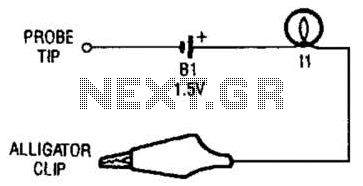
The continuity tester consists of a battery and a lamp connected in series, with one end of the circuit terminated with an alligator clip and the other end connected to the probe tip. The continuity tester is a fundamental...
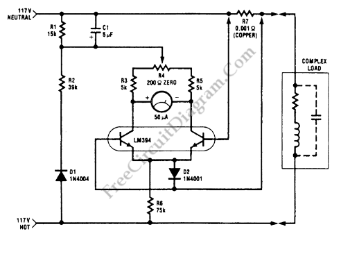
This watt-meter circuit has a measurement range of up to 1 kW. It can provide complete (X)(Y) functionality while utilizing only one transistor. The circuit is designed for operation with 117 Vac ± 50 Vac. Modifications can be made...
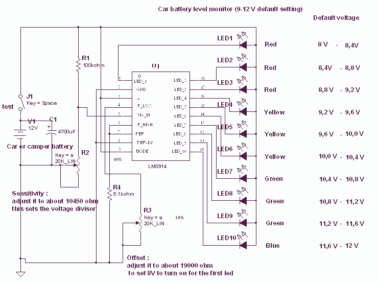
This circuit uses the popular and easy to find LM3914 IC. This IC is very simple to drive, needs no voltage regulators (it has a built-in voltage regulator) and can be powered from almost every source. When the test...
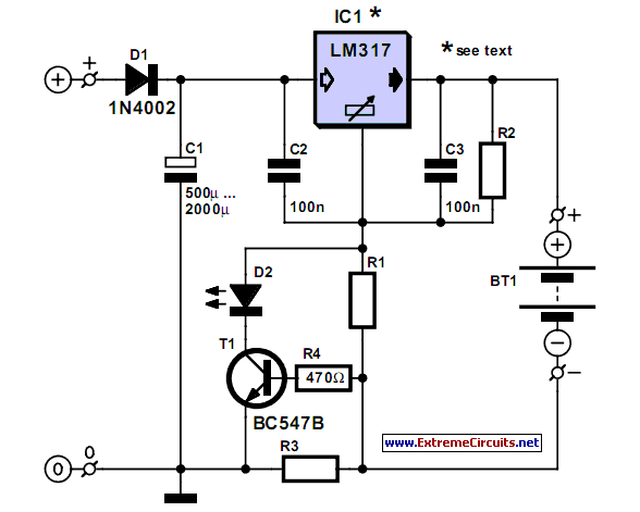
A simple NiCd charger can be constructed using readily available components and an economical LM317 or 78xx voltage regulator. The design incorporates a current limiter made up of resistor R3. The proposed NiCd charger circuit utilizes an LM317 or a...

This NiCd battery charger is capable of charging up to seven NiCd batteries connected in series. The number of batteries can be increased if the power supply voltage is raised by 1.65V for each additional battery. When Q2 is...
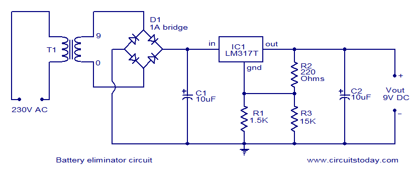
This document presents a circuit diagram of a battery eliminator circuit designed to replace 9V PP3 batteries. It can power any device that operates on a 9V battery. The transformer T1 reduces the mains voltage, while bridge rectifier D1...
Warning: include(partials/cookie-banner.php): Failed to open stream: Permission denied in /var/www/html/nextgr/view-circuit.php on line 713
Warning: include(): Failed opening 'partials/cookie-banner.php' for inclusion (include_path='.:/usr/share/php') in /var/www/html/nextgr/view-circuit.php on line 713