
9V fm transmitter circuit design using transistors
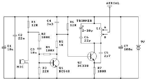
The circuit utilizes a tuned coil, L1, which is integral to the operation of the LC oscillator. The two output taps, A and B, provide flexibility in selecting the desired output characteristics. Tap A is designed for applications requiring a stable low-frequency output, while tap B offers a higher frequency output, albeit with less stability. The selection between these taps allows for adaptation based on the specific requirements of the application, such as range and signal clarity.
The oscillator circuit, formed by L1 in conjunction with capacitors C5 and C6, establishes the resonant frequency of the system. The values of these components must be carefully chosen to achieve the desired operating frequency. The relationship between L1 and the capacitors is critical, as it dictates the tuning range and stability of the oscillator. This configuration is commonly used in RF applications where precise frequency control is essential.
It is important to note that the output power of approximately 2.5 mW indicates that this transmitter is intended for low-power applications. The reduced output level may limit the effective range of transmission, but it contributes to enhanced frequency stability, making it suitable for applications where signal integrity is paramount.
However, one of the inherent challenges of this design is its sensitivity to external loads, particularly antennas. The presence of an antenna alters the impedance seen by the oscillator, which can lead to variations in the resonant frequency. This phenomenon necessitates careful matching of the antenna to the transmitter to minimize frequency drift and ensure consistent performance. Proper tuning and adjustment of the circuit in conjunction with the antenna can mitigate these effects, allowing for optimal operation within the intended frequency range.The tuned coil L1, has two output tapping for the antenna connection, marked "A" and "B". These are both low-level outputs and you choose which tapping you want to use ( stable low range, or more unstable but higher range). Tap B (2. 5%) takes just a very small portion of signal from the oscillator circuit and therefore gives a very frequency stabl
e transmitter. The output level (around 2. 5mW) and range are therefore somewhat reduced. The frequency determining elements (L1, C5 and C6) form a simple LC tuned oscillator. The inherent problem with this type of circuit diagram transmitter is that any external load (antenna) will change the operating frequency. 🔗 External reference
Related Circuits
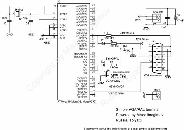
To prevent image distortion when receiving data via UART for VGA, it is advisable to conduct data exchange with the terminal approximately 300-600 microseconds after the vertical synchronization (VSYNC) signal. In a VGA system, the synchronization signals are crucial for...
The multivibrator flashing light emitting diode (LED) display driver circuit can be utilized in toys, creating flashing effects in the eyes of animals or monsters. This circuit employs a multivibrator configuration, typically a 555 timer IC or a similar component,...
The more one understands about any subject, the more interesting it becomes. As this article is read, it will be found that the subject of... A comprehensive electronic schematic typically involves various components, each serving a specific function in the...
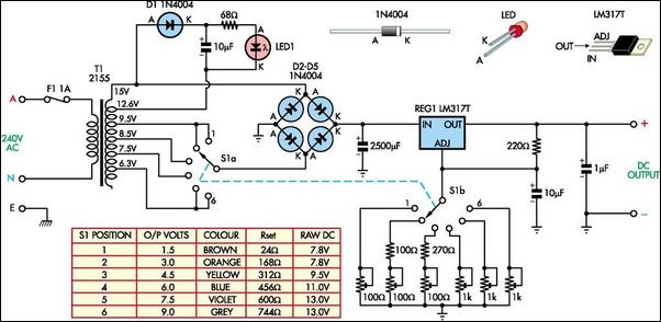
The following circuit illustrates a Battery Replacement Power Supply Circuit Diagram. This circuit is based on the LM317 integrated circuit. Features include the ability to replace... The Battery Replacement Power Supply Circuit utilizes the LM317 voltage regulator to provide a...
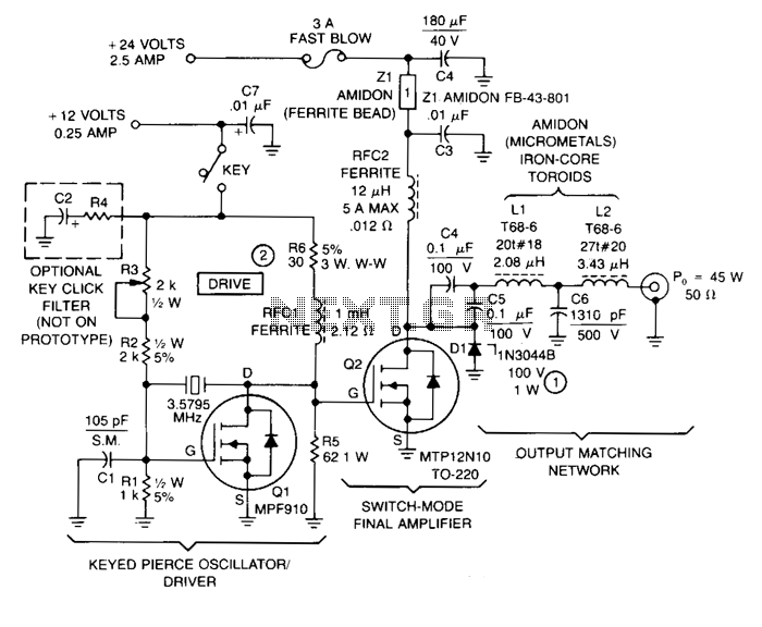
This transmitter comprises a keyed crystal oscillator/driver and a high-efficiency final amplifier, both utilizing a TMOS Power FET as the active component. The total cost of components is under $20, and no specialized construction skills or circuit boards are...
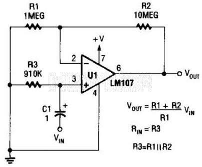
A general-purpose noninverting AC amplifier for audio and other low-frequency applications is presented. Design equations are included in the figure. Almost any general-purpose operational amplifier can be utilized for U1. The circuit configuration features a noninverting amplifier topology, which is widely...
Warning: include(partials/cookie-banner.php): Failed to open stream: Permission denied in /var/www/html/nextgr/view-circuit.php on line 713
Warning: include(): Failed opening 'partials/cookie-banner.php' for inclusion (include_path='.:/usr/share/php') in /var/www/html/nextgr/view-circuit.php on line 713