
A low noise four phase crystal oscillator
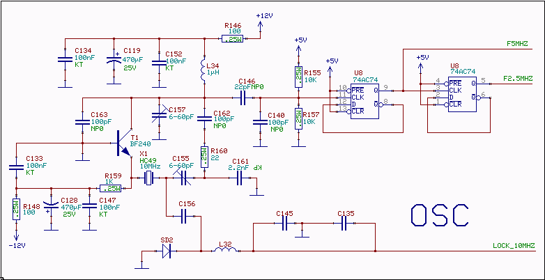
This oscillator circuit is characterized by its ability to maintain low noise levels while providing stable oscillation at the desired frequency. The careful selection of component values, including feedback resistances and capacitive elements, is crucial in achieving the desired performance metrics. The application of a bipolar transistor in a grounded base configuration enables the realization of low input and output impedances, essential for preserving the selectivity of the crystal oscillator. The design considerations reflect a balance between noise performance and oscillation stability, making it suitable for high-performance applications in radio frequency systems. The choice of operating the transistor in class C, despite its drawbacks near the carrier, is a strategic decision aimed at optimizing the overall noise performance at greater frequency separations. This approach is supported by the theoretical understanding of thermal noise behavior in resonant circuits, ensuring that the oscillator meets the stringent requirements of modern communication systems.A 10 MHz crystal is typically 4 ohms at its series resonance and 40 kiloohms at its parallell resonance. To get low sideband noise the power dissipated in the crystal has to be reasonably large, the design used here dissipates 0.
2mW in the crystal, 7mA and 30mV across the crystal. An oscillator can be seen as an amplifier which has feedback throug h a filter. The amplifier of a series resonance oscillator must have both a low input impedance and a low output impedance, preferrably below 4 ohms to preserve the selectivity associated with the high Q of the crystal. The thermal noise in the losses of the crystal is k * T0 = -174 dBm/Hz. With a power dissipation of - 7 dBm the flat noise floor is thus 167 dB below the carrier if we compare the power dissipated in the losses of the quarts to the thermal noise generated by the same losses.
The flat noise floor at the collector side may be a good deal better than this even if the amplifier impedance is matched to, or lower than the resistive part of the crystal impedance. This is because the voltage gain for the thermal noise produced within the crystal drops quickly with the frequency separation since the reactive part of the crystal impedance comes in series with the noisy 4 ohm resistive part.
The noise generated by the transistor itself will be attenuated by the large emitter impedance presented to the emitter by the crystal at frequency separations of a few kHz or more so the flat noise floor may be well below 167 dBc/Hz. The flat noise floor can be made much lower than one would expect from comparing noise power to signal power using the noise figure and feed impedance at the resonance frequency of the crystal.
A termination resistor from emitter to ground may improve the noise close to the carrier but it may degrade the noise floor by more than 10dB at large frequency separations. Everything is inverted. With the same power dissipated in the crystal and the same temperature one gets the same result for an ideal amplifier.
Here the noise voltage generated by the losses in the crystal is shunted by the much lower reactive impedance of the crystal far from the resonance. The parallel resonance oscillator needs an amplifier with an input impedance of at least 40 kiloohms.
To give a good performance close to the carrier, the noise figure has to be low at 40 kiloohms input impedance. To give a low value for the flat noise floor far away from the carrier, the amplifier has to have a low noise figure also at source impedances below 1 kiloohm.
My personal experience with parallel resonance oscillators is not as good as with series resonance ones, that is the reason a series resonance oscillator was chosen as the pure oscillator required in the 2. 5MHz high performance direct conversion receiver. The oscillator has the crystal in series with the emitter of a bipolar transistor. The complete circuit diagram is shown in fig. 1. The input impedance of a grounded base BF240 is about 4 ohms if the transistor is run in class A. The impedance across 4. 7nF is about 3 ohms. Feedback is through 100 ohms of capacitive reactance and 10 ohms of resistive to get feedback in the correct phase.
The 10 ohm resistor is also a load for the output of the amplifier, it dissipates about 30mW of LO power. The design presented here runs the BF240 transistor in class C which results in a very poor performance close to the carrier.
On the other hand, the flat noise floor far from the carrier is very low. See for example the article by Gerhard Hoffmann, DK4XP in Dubus 2/2001 The flicker noise close to the carrier could be reduced by use of a more complex oscillator design but that would only affect performance closer to the carrier than about 1kHz. It would of course improve short time stability also. In my experience, running oscillators in class C may improve the flat noise floor far away from the carrier.
At a carrier frequency of 2. 5 MHz, far a 🔗 External reference
Related Circuits

Low power 5V switching regulator power supply. Visit the corresponding page for an explanation of the related circuit diagram. The low power 5V switching regulator is designed to efficiently convert a higher input voltage to a stable 5V output while...
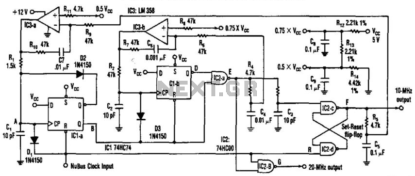
This circuit generates a 20-MHz clock signal that is phase locked to a 10-MHz clock found in the Apple MAC II. To create the 20-MHz output, the circuit generates a 25 ns negative-going pulse that is delayed by 50...
This is a line follower designed to trace grid-type tracks. It features five line sensors for tracking the line. This arrangement of five sensors has proven effective, having been used multiple times with successful results. The device is named...
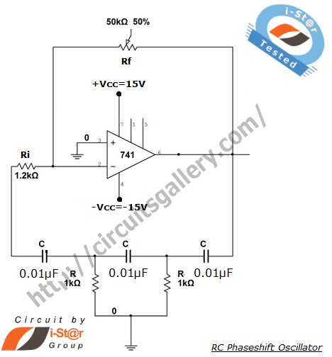
A phase-shifted oscillator can be constructed using a basic operational amplifier (op-amp), three resistors, and three capacitors. One of the resistors should be adjustable, while the other components should have the same value. This oscillator design exhibits low distortion...

The precision Phase Locked Loop (PLL) in this circuit operates similarly to a basic PLL, but with several enhancements. The flip-flops in the detector are equipped with a gate G1 to clear them, allowing for a faster response. The...
The circuit is a standard RC phase shift oscillator that utilizes a single bipolar transistor as the active component. When power is supplied, regenerative feedback is applied through capacitor C2 from the collector to the base of the transistor....
Warning: include(partials/cookie-banner.php): Failed to open stream: Permission denied in /var/www/html/nextgr/view-circuit.php on line 713
Warning: include(): Failed opening 'partials/cookie-banner.php' for inclusion (include_path='.:/usr/share/php') in /var/www/html/nextgr/view-circuit.php on line 713