
A part of product detector circuit composed of LF198 and LM122H
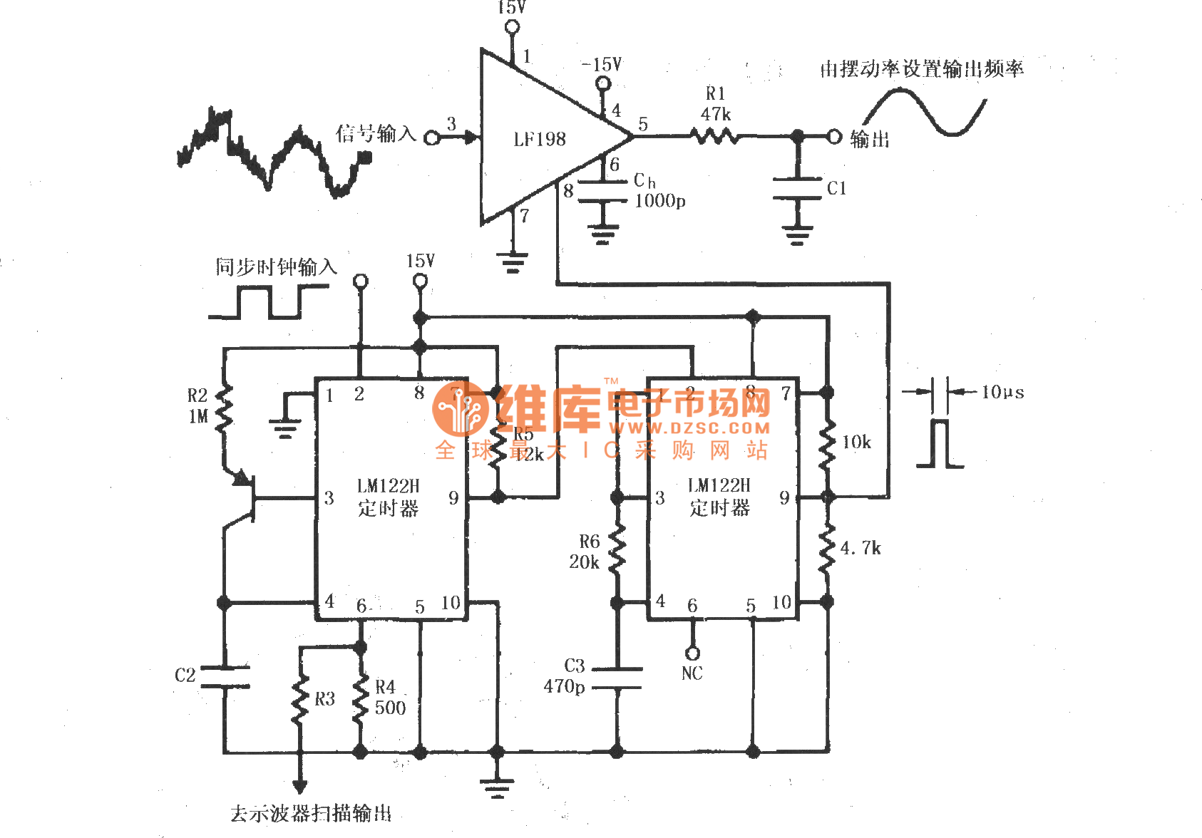
The circuit operates by utilizing two LM122H timer ICs configured in a cascading arrangement. The first LM122H receives the synchronous clock signal and generates a pulse that is subsequently modified by the second LM122H. This configuration allows for precise control over the pulse width, which is critical for applications requiring accurate timing and synchronization.
The LF198 is a sample-and-hold amplifier that is designed to capture and hold the voltage of an input signal for a specified duration. In this setup, the output pulse from the LM122H timers serves as the control signal for the LF198, dictating when the device samples the input signal. The control signal is connected to pin 8 of the LF198, enabling the device to operate effectively in a sampling mode.
It is important to note that the input signal presented to the LF198 at pin 3 may contain various noise components. This noise can adversely affect the performance of the sample-and-hold circuit, potentially leading to inaccurate voltage readings. Therefore, appropriate filtering techniques may be required to clean the input signal before it reaches the LF198. Implementing low-pass filters or other noise-reduction strategies can help ensure that the sampled signal is as clean as possible, thus improving the overall performance of the circuit.
In summary, the described circuit effectively utilizes LM122H timer ICs to generate a controlled pulse width from a synchronous clock signal, which is then used to control the sampling process of the LF198. Careful consideration of noise management is essential for optimal circuit functionality.Synchronous clock signal is input to a cascade of timer circuit composed of two LM122H, then the synchronization clock is converted to the desired width of the pulse (Fig. 10?s) which will be add to LF198 LOGIC end (8 feet) as the sampling and holding control signal. The signal is input LF198`s pin 3. The input signal contains a large number of noise com.. 🔗 External reference
Related Circuits
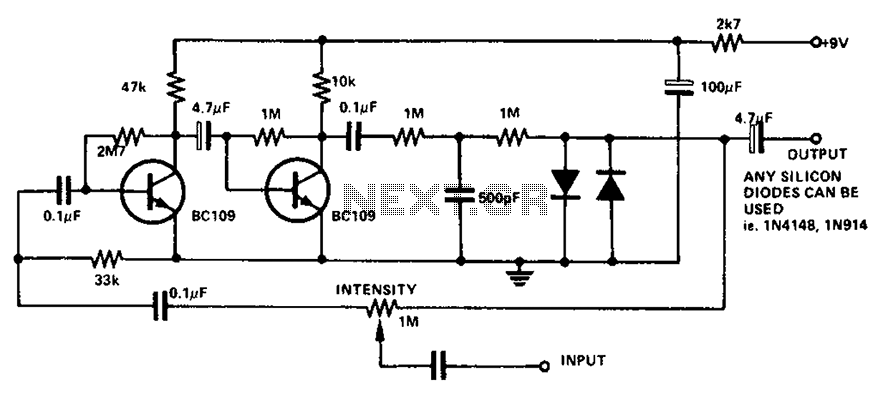
The circuit utilizes a transistor to amplify the input signal. Two diodes are employed to clamp the distorted output, while a 500 pF capacitor filters out high-frequency noise. Under normal conditions, a 1M slide rheostat is used to adjust...
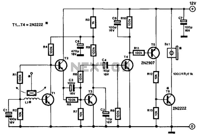
This highly sensitive movement detector is designed using bipolar transistors and operates with a current draw of only 0.3 mA during quiescent conditions. It is primarily intended as a protection device but can also be utilized in specific games....
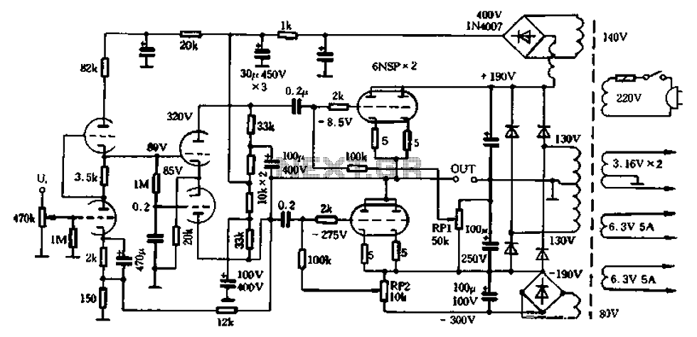
The 6N5P is a low resistance tube with an output impedance of 400 ohms, utilized in a parallel push-pull configuration. The output impedance of a single tube half can be further reduced when employing two or three tubes in...
This circuit functions to monitor the duration of occupancy in a toilet, activating an alert if the time spent exceeds a predefined limit. The components involved include a resistor, integrated circuit (IC), capacitor, and transistor. The occupancy monitoring circuit is...
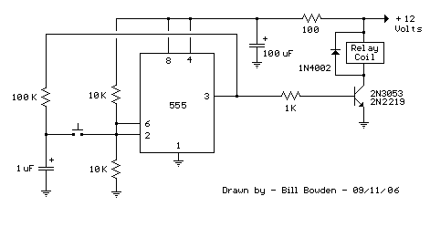
This 555 timer circuit toggles a relay when a button is pressed. Pins 2 and 6, the threshold and trigger inputs, are held at half the supply voltage by two 10K resistors. When the output is high, the capacitor...
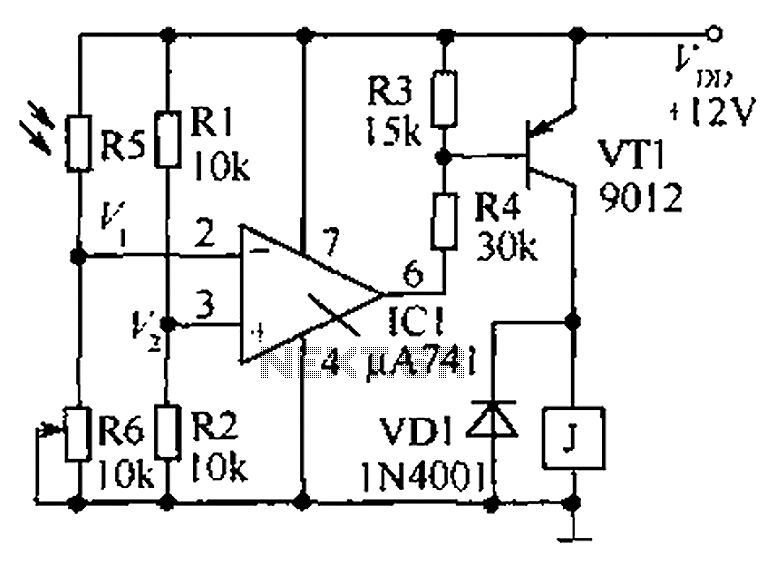
The circuit functions as a precision bright light control circuit, operating independently of variations in power supply voltage and ambient temperature. Resistors R1, R2, R6, and the photosensitive resistor R5 form a two-arm Wheatstone bridge. The precision bright light control...
Warning: include(partials/cookie-banner.php): Failed to open stream: Permission denied in /var/www/html/nextgr/view-circuit.php on line 713
Warning: include(): Failed opening 'partials/cookie-banner.php' for inclusion (include_path='.:/usr/share/php') in /var/www/html/nextgr/view-circuit.php on line 713