
A user friendly boost DC DC converter topology

In designing a DC-DC converter for battery-powered applications, the integration of a frequency compensation circuit is critical for ensuring stable operation across varying load conditions and component tolerances. The use of hysteretic control in buck converters simplifies the feedback loop by leveraging the inductor current ripple information sensed through the capacitor ESR, which inherently stabilizes the output. This approach allows for a responsive adjustment of the switching frequency to accommodate changes in the passive components without the need for complex compensation networks.
For applications requiring voltage step-up, the boost converter architecture presents unique challenges in current sensing and regulation. The implementation of an auxiliary switch (SA) and a separate hysteretic control loop enables precise management of inductor current, ensuring that it remains above the minimum threshold to support load demands. This method enhances the converter's performance by preventing overcharging while maintaining efficiency through asynchronous switching. The design also considers the trade-offs associated with increased inductor current, ensuring that power losses are kept within acceptable limits.
The charge-pump-based duty-cycle-to-voltage demodulator further enhances the control strategy by providing a reliable reference for inductor current regulation. By balancing the charge injected and removed from capacitor C1, the system can maintain a stable voltage reference (VIREF), crucial for the effective operation of the boost converter. Overall, the integration of these techniques results in a robust DC-DC converter solution suitable for a variety of battery-powered devices, optimizing both performance and efficiency.In battery-powered applications, like cell phones, PDAs, digital cameras, etc. , an integrated dc-dc converter circuit solution offers several advantages in terms of cost, size, and design complexity. A critical hurdle in obtaining a fully integrated solution is the frequency compensation circuit, which has to be designed based on the values of external passive filter components
(L-C) and associated parasitic elements, like the capacitor equivalent series resistance (ESR). The values of these off-chip components vary due to manufacturing tolerances, parameter drift, and design requirements. Capacitor ESR can vary by orders of magnitude, based on whether the capacitor is electrolytic or ceramic, not to mention its variation across temperature.
As such, it is required to have a DC-DC controller IC that can provide fast control and stable operation with widely varying passive component values. In hysteretic control for buck converters, the regulated output voltage includes inductor current ripple information sensed indirectly through capacitor ESR, thus simplifying the loop characteristics.
This circuit displays an inherently stable performance and any change in L-C values is accommodated through a change in the converter switching frequency, maintaining stable operation without the use of frequency compensation circuits [1-2]. However, in boost converters, which are used for stepping up single or dual-cell battery voltages for 3.
3 or 5 V applications, the technique is not readily applicable because the inductor current cannot be determined entirely from the output voltage. A strategy that overcomes this limitation in boost converters is presented in Figure 1 [3]. The inductor current, which cannot be determined completely through the capacitor voltage ripple, is independently sensed and regulated through a separate hysteretic loop, containing the main switch SM.
The average inductor current IL is raised above the minimum value required to support load current IO. Starting with a standard boost converter, an additional auxiliary switch SA is added across the inductor L.
When the switch SA is open, the excess inductor current (above the minimum value) tends to charge the capacitor C beyond the desired output voltage. This overcharge is sensed and prevented by comparator Q1, which turns on switch SA and shorts inductor L.
Therefore, the inductor current freewheels, shutting off diode D and letting the capacitor voltage discharge. Switch SA is turned back off when the sensed capacitor voltage VS discharges below reference VREF. The hysteretic problem is thus defined to regulate the output voltage to a desired value between (VIN - VDiode), which is its equilibrium value with switch SA closed, and ID(VOUT/IO), which is its equilibrium value with switch SA open.
This regulation is performed by controlling the duty cycle DA of switch SA. At the appropriate duty cycle DA, the diode current ID, averaged over a switching cycle of SA, equals the load current IO, and average VOUT is stabilized to equal VREF. Switch SA switches asynchronously to switch SM at a much lower switching frequency. The additional power loss due to higher inductor current is kept low by maintaining the inductor current only 5% above the minimum required value (IL_Min).
A representative inductor current reference (VIREF) is derived from duty cycle DA, by means of a charge-pump-based duty-cycle-to-voltage demodulator shown in Fig. 1b. Capacitor C1 is charged and discharged by complementarily switching current sources I1 and I2, which are gated by the controlling signal of switch SA.
The average capacitor current equals zero and the voltage VIREF stabilizes when the total charge injected into the capacitor by I1 during the off time of switch SA balances the total charge removed by I2 during the on time of switch SA. By setting I2 to be 19 times larger than I1, VIREF reaches steady state only when the off t 🔗 External reference
Related Circuits
INTRODUCTION Digital to analog converters are one of the most commonly employed circuits in many applications involving digital video, signal processing, and testing. Digital to analog converters (DACs) serve a critical role in modern electronic systems by converting digital signals,...
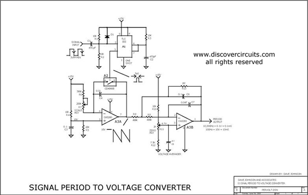
This circuit is designed to convert a square wave input signal into a voltage output. The voltage produced is proportional to the time interval between the edges (period) of the signal, rather than its frequency. The operational range of...
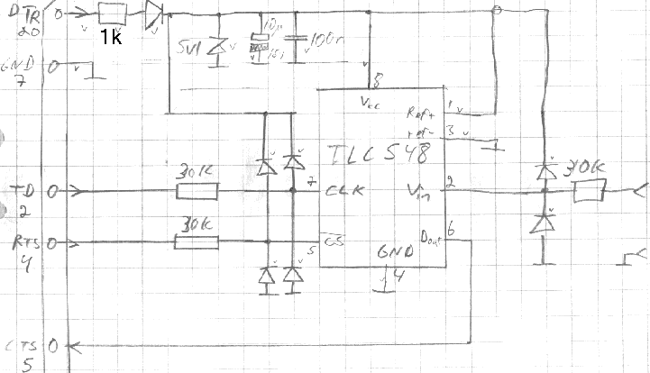
This circuit is a simple 8-bit analog-to-digital converter (ADC) that connects to a PC serial port. It utilizes the TLC548 A/D converter chip, which is known for its serial output. However, the output from the TLC548 is not directly...
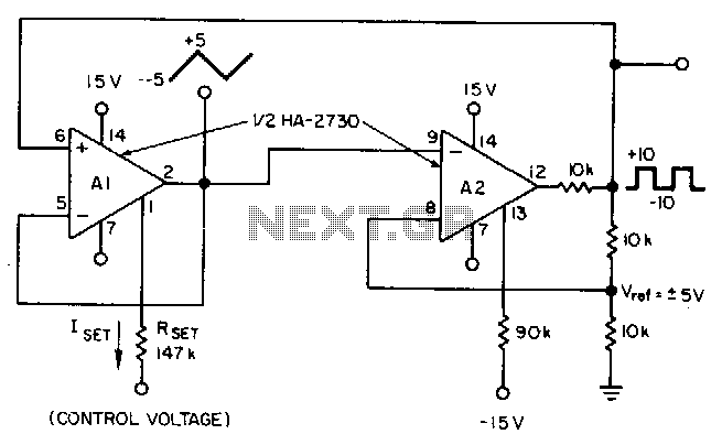
This circuit utilizes a programmable operational amplifier, specifically the HA2730, which is a two-amplifier monolithic chip featuring independent programming ports for each amplifier. The parameters of the amplifiers, including the slew rate, vary linearly based on a set current....
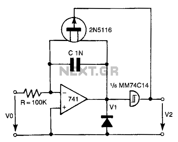
The 741 operational amplifier integrator signal is input into the Schmitt trigger of an inverter. When the signal reaches the positive-going threshold voltage, the inverter's output switches to zero. This output directly controls the FET switch. With a gate...
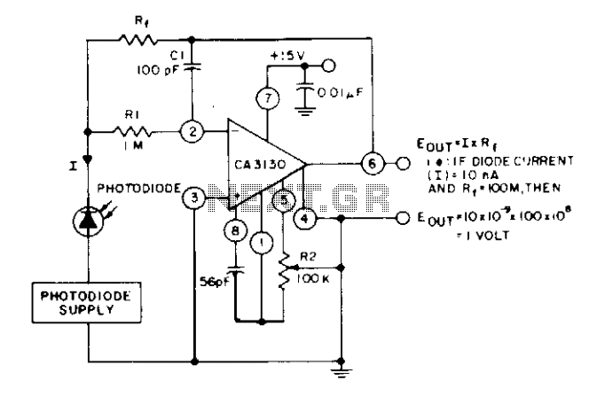
The circuit utilizes three CA3130 BiMOS operational amplifiers in an application that is sensitive to sub-picoampere input currents. It provides a ground-referenced output voltage that is proportional to the input current flowing through the photodiode. The circuit design employs three...