
Absolute-Value Meter With Polarity Detector
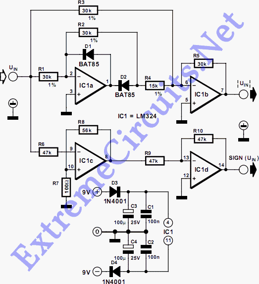
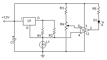
This circuit effectively serves as a versatile tool for signal processing, enabling accurate representation of both the magnitude and polarity of an input voltage. The full-wave rectifier configuration implemented with operational amplifiers IC1a and IC1b ensures that the absolute value of the input signal is consistently provided, regardless of the input's polarity. The design is robust enough to handle a range of input voltages while maintaining output integrity, making it suitable for various applications in signal conditioning and measurement systems.
The choice of operational amplifiers and resistors is critical to the performance of the circuit. Using high-precision resistors (1% tolerance) for R1-R4 minimizes the potential for error in the rectification process. In scenarios where low input voltages are expected, selecting operational amplifiers with low offset voltage characteristics is essential to maintain accuracy. The feedback mechanism in the polarity detection section, facilitated by R7 and R8, introduces hysteresis, which is particularly beneficial in applications where the input signal may fluctuate slowly, ensuring stable output and preventing unintended switching.
The integration of the output signals |Uin| and SIGN into a bi-directional bar display system allows for clear visualization of both the magnitude and sign of the input voltage. This functionality makes the circuit particularly useful in instrumentation and control systems where real-time monitoring of voltage levels is required. The ability to operate both circuits independently or in tandem enhances the circuit's versatility, allowing it to adapt to various electronic applications seamlessly.This circuit breaks an input voltage signal down into its components: (1) the absolute value and (2) the polarity or sign` (+ or ). It will handle direct input voltages as well as alternating voltages up to several kHz. With a supply voltage of ±9 V, the input level should remain below ±6V. The circuit consists of two sections, each having it s own function. Operational amplifiers IC1a and IC1b form a full-wave rectifier, its output terminal supplying the absolute value of the input signal, while operational amplifiers IC1c and IC1d examine the polarity of the input voltage. For negative input voltages, the output of IC1a goes high. Consequently D2 is reverse-biased so that IC1a has no effect on the rest of the circuit. IC1b then acts as an inverter because its amplification is ( R5/R3) or 1. Thus, the output voltage is positive. For positive input voltages, D2 conducts and the amplification of IC1a is -1. The output voltage is then determined by the sum of currents that flow through R3 and R4. Taking into account the polarities and the value of all resistors, the overall amplification becomes This means that the value of the output voltage at the output terminal is the same as the input voltage, but the polarity is always positive.
The accuracy of the rectification process is determined by the accuracy of resistors R1-R4; close-tolerance (1%) types are recommended. At low input voltages (smaller than 20 mV), the input offset voltage of the operational amplifiers may introduce significant errors.
If this is the case, use individual operational amplifiers instead of an array of four (TL061, TLC271, AD548, . ), because they have pins for offset voltage compensation. Alternatively, use an operational amplifier with a low offset voltage like the OP07. In the polarity detector IC1c acts as a comparator, with a certain amount of positive feedback due to R7 and R8.
This feedback causes a hysteresis of 20mV that prevents oscillation when the input voltage changes slowly. IC1d is an ordinary inverter. For input voltages above 10mV, the SIGN output terminal will swing to almost the positive supply. When the input voltage is below 10mV, the SIGN terminal drops low, almost to the negative supply voltage.
For input voltages between these two thresholds, the output voltage is well defined, too, because it stays at its previous level. This circuit is the perfect complement to the +/ voltage on bargraph display` circuit discussed elsewhere in this blog.
The |Uin| and SIGN outputs of the present circuit may be directly connected to Uin and CONTROL IN inputs of the bi-directional bar display. The ±6 V sign indicator signal may be used as the control voltage for the +/ voltage display as long as the reference voltage remains smaller than 3 V.
Although presented as a pair, both circuits may of course be used individually for other purposes. 🔗 External reference
Related Circuits
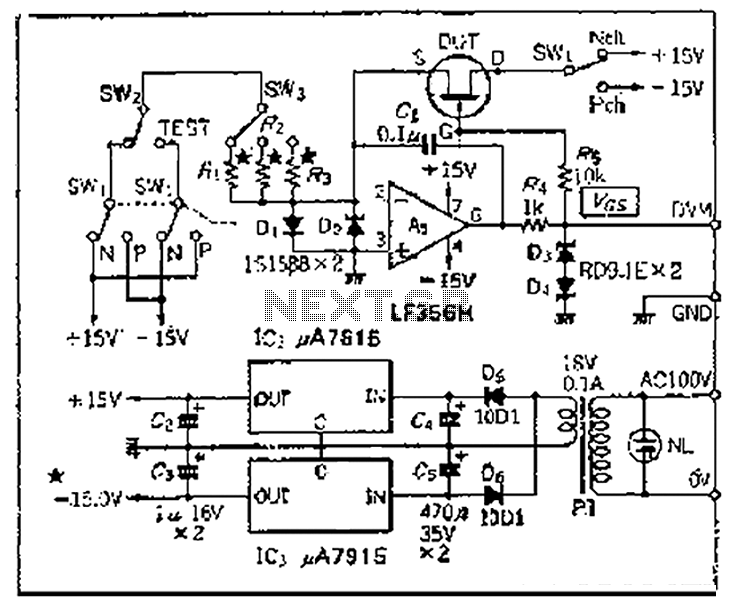
Chen is in the operational amplifier circuit, utilizing a feedback loop with input resistance that determines the current roll-off. The FET drain current is controlled by the determination circuit, which provides the necessary voltage. The output constitutes a fake...
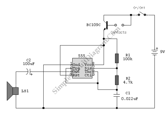
This schematic diagram illustrates a 555 IC water level sensor and detector alarm circuit. The circuit is powered by the emitter current of the BC109C transistor. The 555 timer operates as an astable oscillator in this configuration. Under dry...
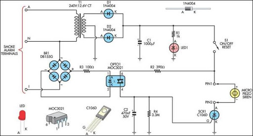
This alarm circuit is designed to monitor a mains-powered smoke detector located in a shed used for dog kennels. It ensures complete isolation from the mains, allowing low-voltage (12V) cabling to run to the alarm circuit, which is situated...
A reverse polarity protection circuit is presented, similar to the one depicted in Figure 2 of SLVA139: Reverse Current/Battery Protection Circuits. The circuit in question is slightly more complex due to the potential input voltage range of 5-40V. Most...
This simple circuit uses an incandescent lamp to detect airflow. With the filament exposed to air, a constant current source is used to slightly heat the filament. As it is heated, the resistance increases. As air flows over the...
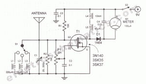
A sensitive and reliable RF field strength meter is an invaluable instrument in amateur radio and in the radio-controlled model area. A field strength meter is. A radio frequency (RF) field strength meter is a specialized device used to measure...