
Adder circuit
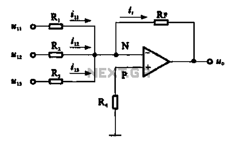
The inverting adder circuit operates based on the principle of superposition. Each input voltage is applied through its respective resistor to the inverting terminal of the operational amplifier. The output voltage (V_out) can be expressed mathematically as V_out = - (R_f/R_i) * (V_1 + V_2 + V_3 + ... + V_n), where R_f is the feedback resistor and R_i represents the input resistors corresponding to each input voltage. The negative sign indicates that the output is inverted relative to the input signals.
In the typical configuration, the operational amplifier's inverting input is connected to the junction of the input resistors. The feedback resistor R_f connects from the output back to the inverting input, creating a feedback loop essential for the operation of the amplifier. The non-inverting input is typically grounded or connected to a reference voltage, ensuring stability in the circuit.
The balancing resistor R4 plays a critical role in maintaining the correct gain and stability of the circuit. Its value is chosen to match the equivalent resistance of the input resistors to minimize offset errors and ensure accurate summation of the input signals. The design allows for flexible scaling of the output voltage by adjusting the feedback and input resistors, thus enabling the circuit to accommodate a variety of applications, such as audio mixing, signal processing, and data acquisition systems.
Overall, the inverting adder circuit is a fundamental building block in analog electronics, providing a straightforward method for summing multiple voltage signals while maintaining control over the gain and phase characteristics.Adder circuit commonly used inverting input, namely the inverting adder circuit. It was to the inverting input of the operational amplifier electrical path, based on the signal voltage to be added through a resistor connected to the inverting input terminal of the operational amplifier. Adder circuit shown in Figure 7-5, which is having a three input inverting adder circuit. Wherein the input signal number eight ii, machine 2,1113 are N input from the inverting input terminal, pin feedback resistors, non-inverting input terminal P via the balancing resistor R4 connected to.
The resistance value of the balancing resistor R4 vase should be Ri, R2, R3 and the parallel and Rr. The output voltage of adder circuit input voltage is equal to the sum of the branch, which kind of structure can be realized adder plurality of input signals.
Related Circuits

A voltage-controlled oscillator (VCO) operates similarly to a voltage-to-frequency converter (VFC). Its output frequency is determined by a control voltage input. In the circuit diagram, 'd' represents the amplifier input voltage, which is set to 0.6V, while 'h' denotes...
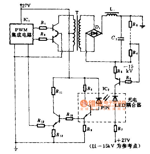
The technical parameters of high-speed optocouplers include a rise time (t1) of less than or equal to 300 ns, a circuit transfer ratio (CTR) of 50%, an isolation voltage (VSO) of at least 15,000 V, and an output transistor...
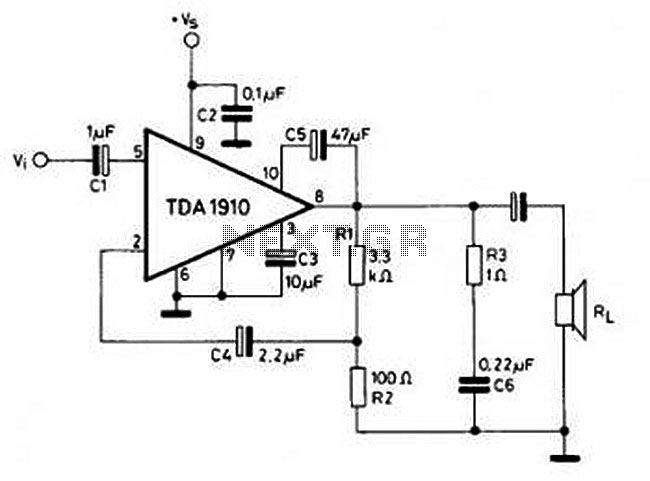
This circuit is simple and inexpensive, which is its primary advantage. Although the output power is not high, the audio quality is good due to the TDA1910's low noise characteristics. This circuit is suitable for use as a student...
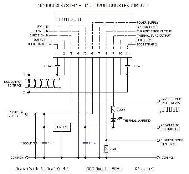
This page features H-Bridge circuits used for controlling direct current motors. Several designs are shown using both CMOS and Bi-Polar power devices. These circuits could be used as the basis for Model Railroad DCC Boosters or PWM motor controllers....
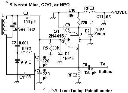
Figure 1 illustrates the VFO oscillator circuit operating within the frequency range of 10.58 to 10.74 MHz. This circuit is a redesigned version of a previously presented Colpitts oscillator, with a clearer representation. The inductor, labeled "L," has an...
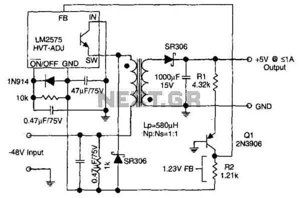
The circuit supplies 1 A at +5 V from the -48 V supply commonly used in telephone equipment. More: The National Semiconductor LM2575 is a simple switching regulator. The circuit utilizes the National Semiconductor LM2575, which is a step-down (buck)...
Warning: include(partials/cookie-banner.php): Failed to open stream: Permission denied in /var/www/html/nextgr/view-circuit.php on line 713
Warning: include(): Failed opening 'partials/cookie-banner.php' for inclusion (include_path='.:/usr/share/php') in /var/www/html/nextgr/view-circuit.php on line 713