
ADUC832 1.3MIPS 8052 MCU + 62kB Flash + 8-Ch 12-Bit ADC + Dual 12-Bit DAC
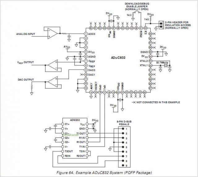
The ADUC836 MicroConverter represents a significant advancement in integrated data acquisition systems, combining the functionality of analog-to-digital (A/D) and digital-to-analog (D/A) conversion along with a microcontroller in a single package. This integration facilitates compact design solutions for applications requiring precise data processing and control.
The device's compatibility with the ADuC816 ensures a smooth transition for users upgrading from previous models, minimizing the need for redesign efforts. The availability of both 52-pin PQFP and 56-pin CSP packages provides flexibility in design, allowing engineers to select the optimal footprint for their specific application needs.
Operating on a dual voltage of 3V or 5V enhances the versatility of the ADUC836, making it suitable for a wide range of applications, from battery-powered devices to more robust systems. The use of a 32 kHz crystal oscillator, paired with an on-chip phase-locked loop (PLL), enables the generation of a stable high-frequency clock at 12.58 MHz, which is essential for maintaining precise timing in data acquisition processes.
The programmable clock divider further enhances the device's flexibility, allowing designers to tailor the microcontroller core clock frequency to meet the requirements of their application. The 8052 core architecture ensures that existing 8051 code can be utilized without modification, thus streamlining development processes and reducing time-to-market.
In summary, the ADUC836 MicroConverter is a powerful and versatile solution for modern data acquisition needs, providing high precision, backward compatibility, and a range of operational features that cater to diverse electronic applications.The ADUC836 MicroConverter is a fully integrated 16-bit data acquisition system-on-a-chip. Like all of ADI`s MicroConverter products, it features precision A/D & D/A conversion and a Flash Microcontroller on a single chip. The ADUC836 is 100% backward compatible (hardware and software) with the ADuC816. It is available in 52-pin PQFP or 56-pin CSP packages and operates on a 3V or 5V power supply. The device operates from a 32 kHz crystal with an on-chip PLL generating a high frequency Clock of 12. 58 MHz. This Clock is routed through a programmable Clock divider from which the MCU core Clock operating frequency is generated.
The Microcontroller core is an 8052 and therefore 8051 instruction set compatible with 12 core Clock periods per machine cycle. By Analog Devices, Inc. 🔗 External reference
Related Circuits
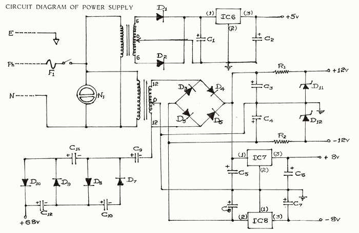
Every electronic device primarily requires a DC power supply for operation. This is a fundamental requirement for any construction project. Consequently, there is a need to obtain multiple voltage values for cost efficiency, convenience, and compact arrangement in various...
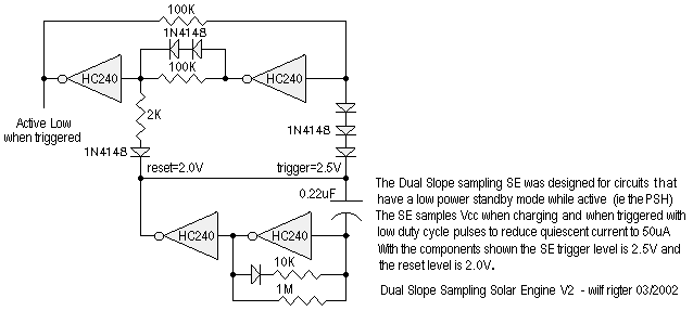
If time was spent experimenting with the ALF type SE circuit, some shortcomings related to a Power Smart Head adaptation may have been discovered. The issue arises because HCMOS gates consume significant power when utilized as SE voltage comparators,...
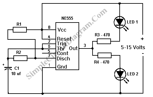
An LED flasher circuit can be constructed using a 555 integrated circuit (IC). The use of the 555 IC allows for greater flexibility in adjusting the flashing rate of the LED. This LED flasher circuit is similar to other...
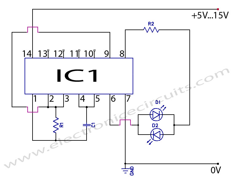
Two LED CMOS Flasher Circuit Diagram. This is a simple two LED CMOS robot (flasher, multivibrator) circuit using CD4069 six inverters. The two LED CMOS flasher circuit utilizes the CD4069 integrated circuit, which contains six inverters, to create a multivibrator...
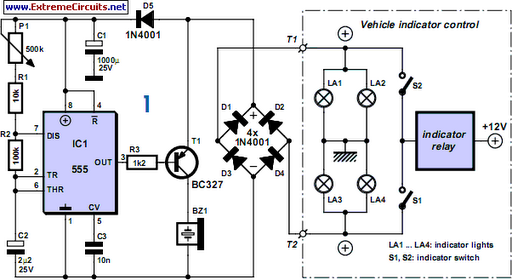
For bikers or scooter riders, it is easy to forget to cancel flashing indicators after turning without an audible reminder. Constantly checking indicator lamps is not practical; attention should remain on the road. The circuit presented here offers an...
When a gas leak occurs, a gas leak alarm must detect the problem immediately and issue an alarm. The gas detection sensor typically used in these types of alarms sends an amplified signal from the sensor to the controlling...
Warning: include(partials/cookie-banner.php): Failed to open stream: Permission denied in /var/www/html/nextgr/view-circuit.php on line 713
Warning: include(): Failed opening 'partials/cookie-banner.php' for inclusion (include_path='.:/usr/share/php') in /var/www/html/nextgr/view-circuit.php on line 713