
AM radio rf amplifier
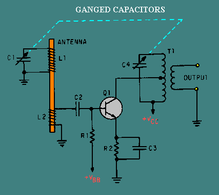
The RF amplifier circuit described is a crucial component in the functioning of AM radio receivers, enabling the amplification of weak radio frequency signals captured by the antenna. The antenna (L1) is designed as a coil, which, along with the variable capacitor (C1), forms a resonant LC circuit. This configuration allows for selective tuning to the desired radio frequency by adjusting the capacitance of C1, ensuring that only the intended signal is amplified.
The coupling of the input signal to the transistor (Q1) is achieved through capacitor (C2), which blocks any DC component while allowing the AC signal to pass. This ensures that the transistor operates in its active region, where it can effectively amplify the incoming RF signal. The biasing of Q1 is critical for its operation; R1 provides the necessary base bias from the power supply (VBB), while R2 sets the emitter bias, ensuring that the transistor remains in the correct operating state. Capacitor (C3) is included to bypass R2, effectively stabilizing the gain and improving the frequency response of the amplifier by providing a low-impedance path for AC signals.
The load for Q1 is formed by the primary winding of transformer (T1) and capacitor (C4), which together create another LC circuit. This load circuit is also tuned by C4, which is mechanically linked to C1, allowing for simultaneous tuning of both circuits. This dual tuning mechanism enhances the performance of the receiver by maintaining optimal impedance matching and maximizing power transfer. The center-tapped configuration of T1's primary winding is particularly important for ensuring that the impedance seen by Q1 is matched appropriately, thereby enhancing the overall efficiency and performance of the amplifier circuit.
In summary, this RF amplifier circuit exemplifies a well-designed system for AM radio reception, incorporating essential elements such as resonant circuits, proper biasing, and impedance matching to achieve effective signal amplification and tuning.a typical rf amplifier that is used in an AM radio receiver. In figure 2-19, the input circuit is the antenna of the radio (L1-a coil) which forms part of an LC circuit which is tuned to the desired station by variable capacitor C1. L1 is wound on the same core as L2, which couples the input signal through C2 to the transistor (Q1).
R1 is used to provide proper bias to Q1 from the base power supply (VBB). R2 provides proper bias to the emitter of Q1, and C3 is used to bypass R2. The primary of T1 and capacitor C4 form a parallel LC circuit which acts as the load for Q1. This LC circuit is tuned by C4, which is ganged to C1 allowing the antenna and the LC circuit to be tuned together. The primary of T1 is center-tapped to provide proper impedance matching with Q1. 🔗 External reference
Related Circuits
Cl. C2 ARCO #462, 2 to 60 pF, trimmer capacitors Li, 3 turns of #20 AWG wire on 1/4" diameter L2, β turns of #20 AWG on 1/4" diameter Ti. Additionally, there is 1 turn of 25 Ω coax...

This circuit is a robust and efficient power amplifier suitable for various audio applications. It delivers 60W RMS output at a 50V supply with an 8 Ohm load. The design is user-friendly, allowing for the use of non-critical components...

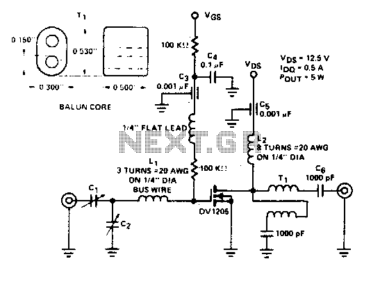
The 2N5485, which has a very low-capacity legacy, is always operated as a source follower with gate bias bootstrap. In this circuit, nothing is left to chance in reducing input capacitance. The 2N5485 is a JFET (Junction Field Effect Transistor)...
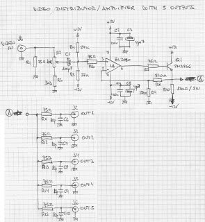
The circuit presented here has numerous applications. Essentially, the distribution amplifier receives a composite video signal from a video player (VCR) or a video generator (analog output) and buffers it, allowing it to be simultaneously sent to up to...
This project involves a 250mW RF power amplifier circuit. It is designed to amplify the output of approximately 7mW wideband FM transmitters to a final output level of about 250mW. The circuit utilizes a simple two-transistor VHF power amplifier...

Floating the grid above ground is detrimental for RF performance and arc protection. The connection of the control grid to ground is critical for stability. It is essential to keep the grid connection to ground as wide and short...