
Analog multiplier

The described circuit utilizes a frequency-to-voltage (F-V) converter and a voltage-to-frequency (V-F) converter, both of which are synchronized by a shared clock signal generated by the LTCIG43. This synchronization ensures that the output frequency of the F-V converter directly corresponds to the input voltage level, while the V-F converter translates this frequency back into a voltage level.
In practical applications, this configuration is essential for systems requiring precise frequency measurement and control, such as in digital signal processing or communication systems. The F-V converter takes an input frequency and converts it into a proportional voltage, which is then fed into the multiplier. The output of the multiplier is influenced by the voltage from the V-F converter, which serves to maintain the stability and accuracy of the system.
Calibration of the circuit is a critical step to ensure precision in operation. By shorting the X and Y inputs to a specific reference voltage of 1.7320 V, the circuit can be fine-tuned. This adjustment is made to achieve a precise output of 3 V, which may represent a standard reference level for subsequent processing stages. The calibration process may involve using a variable resistor or potentiometer to adjust the gain of the multiplier, ensuring that the output remains consistent under varying input conditions.
Overall, this circuit configuration is a robust solution for applications requiring accurate frequency-to-voltage and voltage-to-frequency conversions, with the calibration process allowing for fine-tuning to meet specific operational requirements.The F — V input frequency is locked to the V — F output because the LTClG43's clock is common to both sections. The F — V's reference is used as one input of the multiplier, while the V — F furnishes the other.
To calibrate, short the X and Y inputs to 1.7320 V and trim for a 3-V output.
Related Circuits
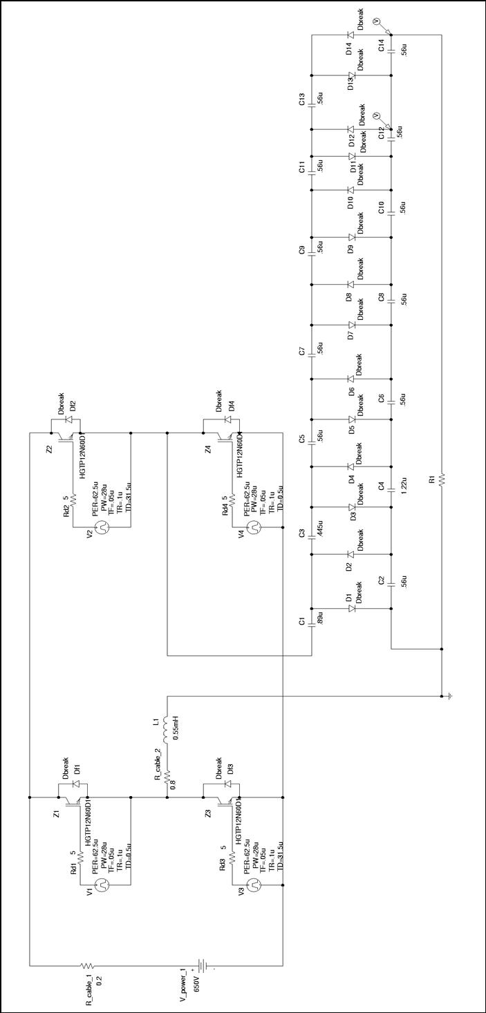
Thesis by Rafael Bräg at the University of Canterbury, New Zealand, in cooperation with the Universität Karlsruhe, Institut Elektrotechnik und Hochspannungstechnik. The thesis presents a comprehensive study conducted by Rafael Bräg, focusing on advancements in the field of electrical engineering....
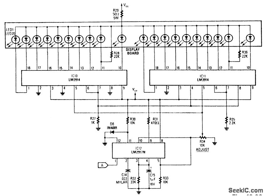
The analog display includes a frequency-to-voltage converter (IC12) along with bar-graph segment drivers IC10 and IC11. The calibration adjustment resistor R34 is configured to ensure that an engine speed of 5000 to 7000 rpm activates the first LED, which...
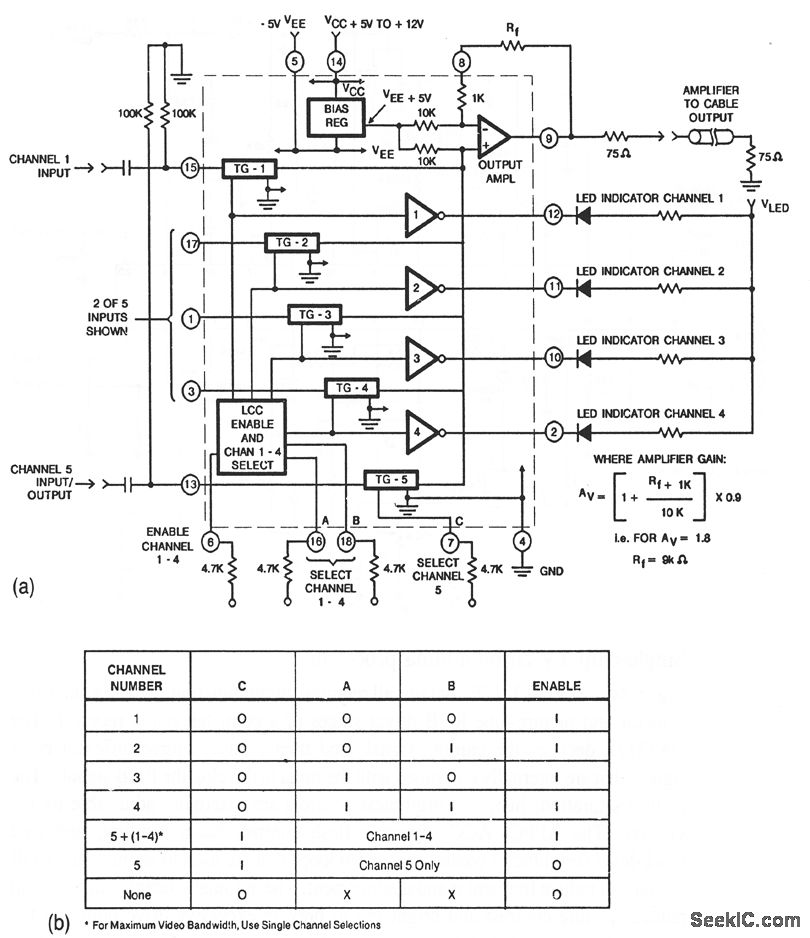
This circuit illustrates a CA3256 switch/amplifier configured for a direct-coupled output. One of four channels can be selected in parallel with channel 5. The analog switches of channels 1 to 4 are digitally controlled by logic. A VEE of...
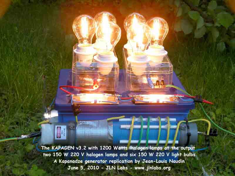
The purpose of the Kapagen is to suck the free electrons from the Earth. The Earth is a big capacitor which contains free electric charges. If it is possible to create or to find a potential imbalance between two...
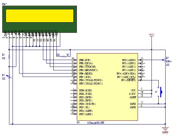
A straightforward tutorial on utilizing the ADC (Analog to Digital Converter) unit of the AVR microcontroller, demonstrated with the Atmega8, including a circuit diagram and code examples. The ADC unit in the Atmega8 microcontroller is a crucial component that allows...
Build an interface board to connect scientific equipment, specifically a pair of photovoltaic tubes, to a personal computer for acquiring measurement results. The signal properties include two channels with a common ground, a one-second acquisition time, and a maximum...