
Analog switches carrier suppression amplitude modulation circuit
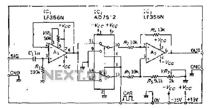
The circuit employs an analog switch configured as a double loop, double-break mechanism, which allows for precise control over the modulation process. The differential modulation amplifier serves to amplify the input modulation wave while ensuring that the signal remains within the desired amplitude limits. This configuration is critical for applications requiring high fidelity in signal transmission.
The carrier control switch is responsible for managing the timing of the modulation. It is designed to switch between different states, ensuring that the modulation wave is inverted at the appropriate intervals. This inversion is crucial for achieving the desired amplitude modulation characteristics, where the carrier signal's polarity is reversed without introducing distortion.
The circuit's operation is contingent upon maintaining a stable carrier frequency. Analog switches, while effective for low-frequency applications, are limited in their performance at high frequencies. Therefore, careful consideration must be given to the selection of components to ensure that the analog switch can handle the required frequency range without degradation of the signal quality.
The output of the modulation process is a square wave, which inherently contains high-frequency harmonics. To refine this output into a more desirable sine wave form, a band-pass filter is integrated into the circuit. This filter is tailored to allow only the desired frequency components to pass through while attenuating unwanted high-frequency noise, thereby enhancing the overall signal integrity.
In summary, this circuit design effectively combines an analog switch and a differential modulation amplifier to achieve controlled amplitude modulation. The incorporation of a band-pass filter further ensures that the output signal meets the required specifications for sine wave characteristics, making this configuration suitable for various electronic applications.Analog switch (double loop, double-break) and differential modulation amplifier complete the work. The carrier control switch, switch contacts in the time, from the inverting i nput Chi input modulation wave is inverted. Back when the next carrier-inverting input, so that the anti- re going, to achieve the limit amplitude modulation, the carrier will not braid week and intermittent, but the polarity reversal. Analog switches must keep the carrier frequency, at high frequencies can not use. The modulated output is crossing the square, containing high frequency changed as needed to increase the band-pass filter, to obtain a sine wave signal.
Related Circuits
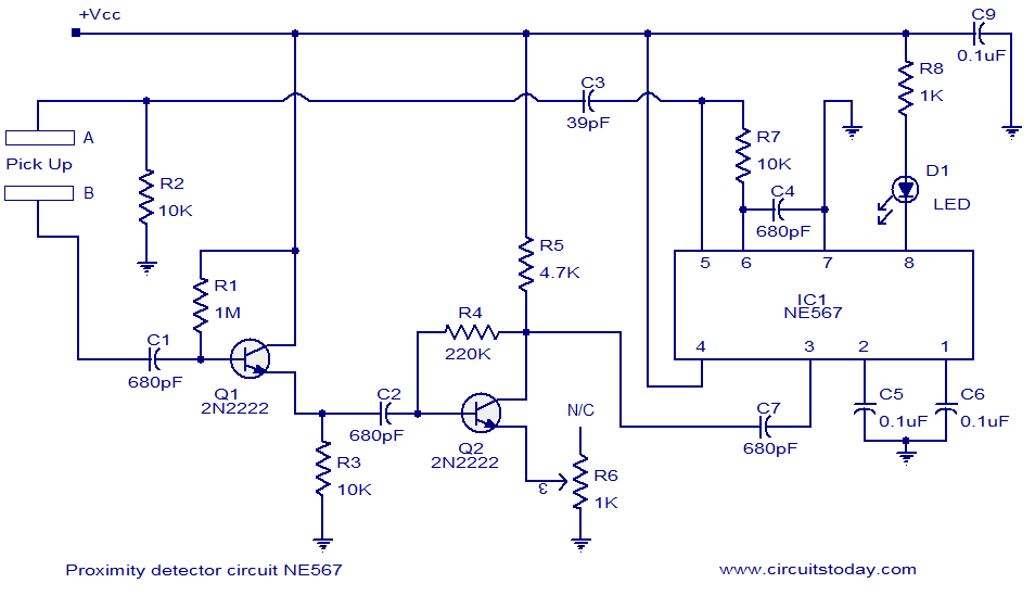
A simple proximity detector circuit utilizing the NE567 integrated circuit (IC). The circuit activates an LED when an object approaches the sensor. The NE567 is a versatile phase-locked loop (PLL) device commonly used for applications such as proximity detection due...
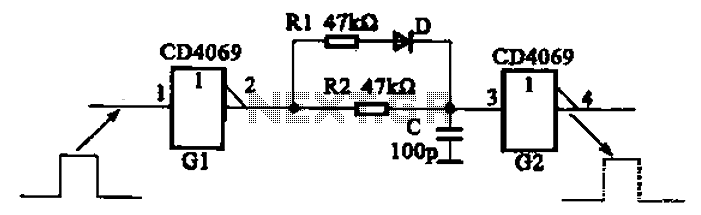
The inverter circuit using CD4069 is configured with a delay and width adjustment. When the output of the inverter (G1) is high, the capacitor (C) charges through resistor (R1) and diode (D). The voltage across capacitor C quickly reaches...
Just point this small device at the TV and the remote gets jammed. The circuit is self-explanatory. 555 is wired as an astable multivibrator for a frequency of nearly 38 kHz. This is the frequency at which most of...
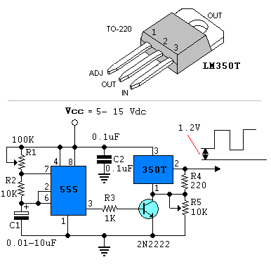
Power pulse circuit using LM350 and NE555. This circuit can be used to drive lamps, power LEDs, DC motors, etc. Adjust R5 for output amplitude and R1 for output power. The LM350 is an adjustable 3-terminal voltage regulator. The power...

This is a preamplifier circuit and switching schematic for the Marantz Model 33. The Marantz Model 33 preamplifier circuit is designed to amplify low-level audio signals from various sources before sending them to a power amplifier. The schematic typically includes...
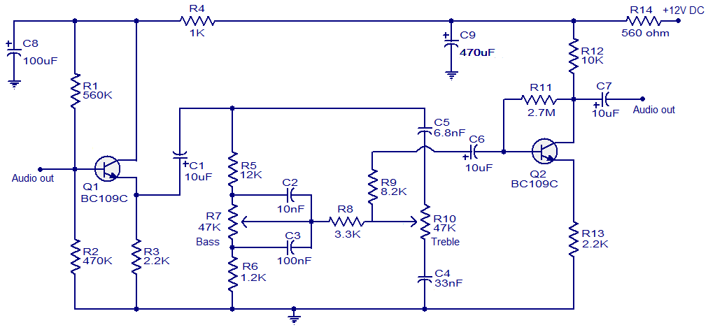
This simple tone control circuit is designed based on the renowned Baxendall tone control circuitry. The circuit can provide a maximum cut or boost of approximately 12 dB at both 10 kHz (treble) and 50 Hz (bass). Additionally, both...
Warning: include(partials/cookie-banner.php): Failed to open stream: Permission denied in /var/www/html/nextgr/view-circuit.php on line 713
Warning: include(): Failed opening 'partials/cookie-banner.php' for inclusion (include_path='.:/usr/share/php') in /var/www/html/nextgr/view-circuit.php on line 713