
Analog Tachometer Readout

The analog display circuit utilizes a frequency-to-voltage converter (IC12) to translate the engine RPM into a corresponding voltage level. This voltage is then processed by two bar-graph segment drivers (IC10 and IC11), which control a series of LEDs to visually represent the engine's performance. The output of IC12 is proportional to the frequency of the input signal, allowing for a direct correlation between engine speed and the displayed output.
Calibration of the circuit is achieved through the resistor R34, which adjusts the sensitivity of the system. By setting R34, the circuit can be fine-tuned to ensure that the first LED in the bar graph lights up at the desired RPM range of 5,000 to 7,000. This redline indicator serves as a visual cue for the operator, alerting them when the engine is approaching its maximum safe operating speed.
The circuit design may also include additional components such as bypass capacitors for noise reduction, and decoupling capacitors to stabilize the power supply to the integrated circuits. Proper layout considerations should be taken into account to minimize interference and ensure accurate readings. The use of appropriate LED drivers can enhance the brightness and visibility of the display under various lighting conditions. Overall, the combination of IC12, IC10, IC11, and R34 creates a robust analog display system for monitoring engine performance. The analog display consists of a frequency/voltage converter (IC12) and bar-graph segment drivers IC10 and IC11.
R34 is the calibration adjustment and is set so that an engine rpm of 5 000 to 7000 rpm lights the first LED (redline value).
Related Circuits
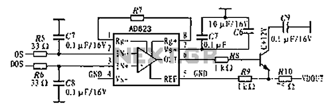
The AD623 is an integrated 3-way amplifier that can operate with either a single or dual supply. It features high common-mode rejection ratio (CMRR) and low voltage drift, along with programmable gain control via an external resistor. All components...
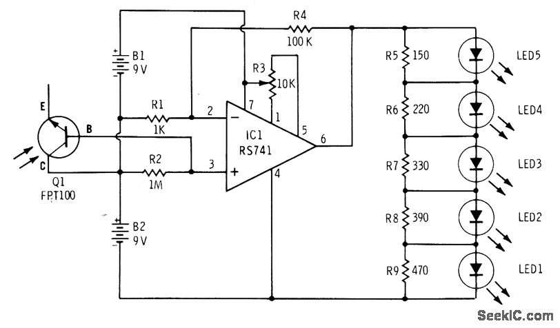
The phototransistor Q1 (Radio Shack 276-130) activates a voltage change across resistor R2, which is then amplified by an operational amplifier (op-amp). The output from the op-amp drives an array of five LEDs, creating a bar graph voltage indicator....
The objective of the project is to design an imager chip for laser-scanned 3-D depth/range finding. The project is divided into two modules: Pixel Array/Centroid Detection and Analog-to-Digital Conversion (ADC). The pixel array/centroid detector tracks the centroid of the...
This circuit is designed to drive a total of 42 LEDs, assuming a forward voltage of approximately 2.2V per LED and a forward current of around 21mA for adequate brightness. If the specifications of the LEDs differ significantly, modifications...
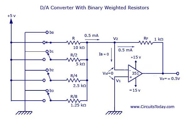
A digital-to-analog (D/A) converter utilizing binary-weighted resistors is illustrated in the accompanying figure. In this circuit, the operational amplifier (op-amp) is configured in inverting mode, although it may also be arranged in non-inverting mode. The schematic represents a 4-bit...
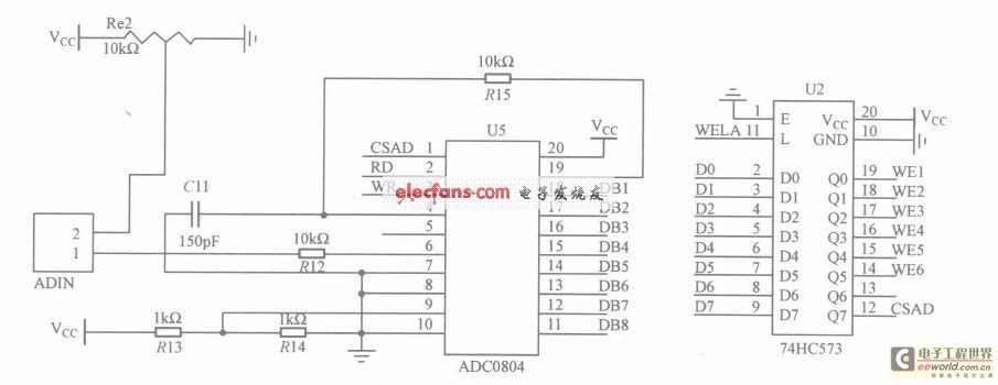
The circuit utilizes the ADC0804, which is configured for left-handed operation, alongside the 74HC573 latch, which is configured for right-handed operation. The latch is connected to a microcontroller, but they are not drawn in the same schematic. The CSAD...