
Analogs ADP1821 Step Down DC-to-DC Converter
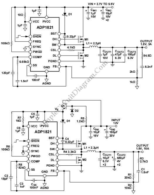
The ADP1821 Step Down DC-to-DC Converter circuit is designed to efficiently convert a higher input voltage into a regulated lower output voltage while maintaining load current capability. The selection of MOSFETs is crucial; they must be rated for the maximum load current and have low on-resistance (RDS(on)) to minimize conduction losses. The dual-channel MOSFETs in the PowerPAK® SO-8 package not only save board space but also facilitate thermal management due to their efficient heat dissipation characteristics.
The circuit configuration is optimized for both performance and cost, employing multilayer ceramic capacitors for their low equivalent series resistance (ESR) and high ripple current ratings, which are essential for applications with significant load transients. The choice of Sanyo OSCON capacitors further enhances performance by providing stability under varying load conditions.
The input voltage range of 2.5 V to 20 V allows the circuit to be versatile across different applications, while the 5 V bias supply is essential for the internal operation of the ADP1821. The use of an external LDO to step down the input voltage to the required levels ensures that the ADP1821 operates within its specified voltage range, thereby enhancing reliability.
In summary, this circuit exemplifies a robust design for a DC-to-DC converter, emphasizing the importance of component selection and layout considerations to achieve optimal performance in high-current applications. The design's flexibility in accommodating various input voltages and load requirements makes it suitable for a wide range of electronic applications, from consumer electronics to industrial systems.Schematic diagram below shows an ADP1821 Step Down DC-to-DC Converter circuit. This circuit uses ADP1821 that can be used to regulate an output with a load of more than 20 A. It can be done if he power components like MOSFETs, the bulk capacitors and the inductor are chosen carefully to achieve the power requirement. The power-train component limi ts the power dissipation and the maximum load. To deliver the 20A load, the two low-side MOSFETs are required. Here is schematic diagram of the circuit: An output load of less than 1A can be driven by The ADP1821. First circuit is a typical application circuit that can drives a 3 A load in an all multilayer ceramic capacitor (MLCC) solution.
Two MOSFETs used in this are dual-channel MOSFETs in a PowerPAK ® SO-8 package. It can save layout space and reduce the cost. The ADP1821 can also be used with an input voltage higher than 5. 5 V. The second circuit is a typical application circuit that operates from a 12 V input. To power the ADP1821, the input voltage must be stepped down by using external LDO, a 5. 6 V Zener diode, a resistor, and an NPN. the LDO that can be used for for input voltages up to 12 V is the ADP3330 or ADP3300. these external signal components are small in size and inexpensive. The circuit require two power rails, they are a power input rail, with range from 2. 5V to 20V and a 5 V bias supply that needs to supply about 30 mA to power the ADP1821 at full load. This circuit uses Sanyo OSCON capacitors as bulk output and input capacitors because it has high current ripple rating and low ESR. Aluminum electrolytic capacitors and the polymer aluminum capacitors can used to replace the OSCON capacitors.
If aluminum electrolytic capacitors are used, they must be paralleled up at the input or output to meet the current ripple requirement. To suppress the current ripple and reduce the effective ESR, a larger bulk input and output capacitance is required because the aluminum electrolytic capacitors have much larger variation in capacitance over the operating temperature range and higher ESR.
[Circuit`s schematic diagram source: analog. com] 🔗 External reference
Related Circuits
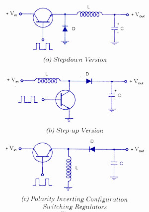
Switching voltage regulators include step-up, step-down, and polarity-inverting configurations, along with their working principles and circuit diagrams. Switching voltage regulators are essential components in modern electronic circuits, providing efficient voltage conversion. These regulators can be categorized into three main types:...
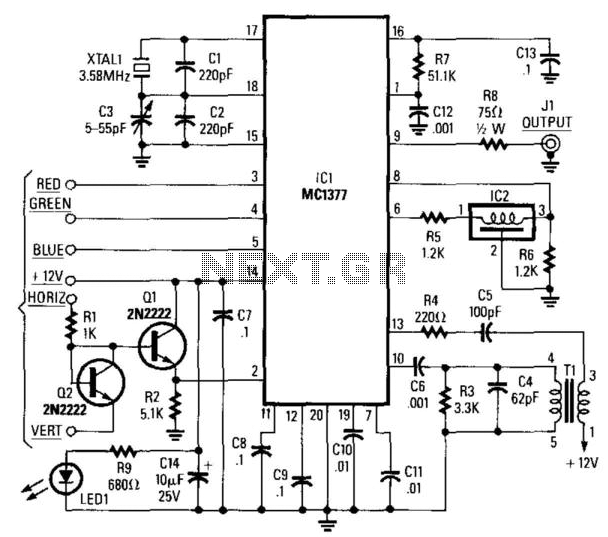
This circuit utilizes a Motorola MC1377 to generate NTSC video from an RGB source. The components are not critical, with the exception of resistor R7, which should have a tolerance of 1%, and capacitor CB, which should have a...
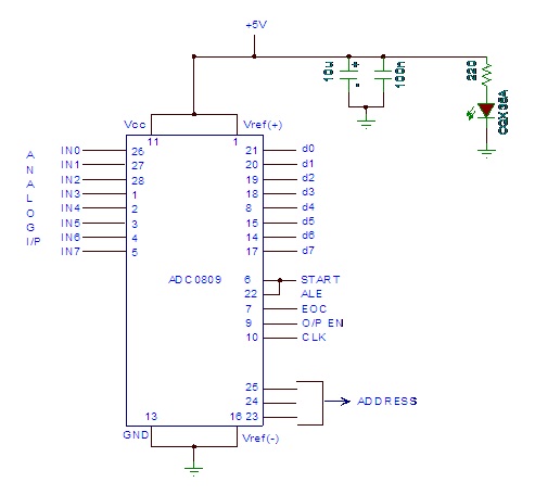
Analog to digital converter modules are utilized in microcontroller-based projects where analog signals need to be transformed into digital signals for further processing in a microcontroller. The integrated chip employed for this purpose is the ADC 0809. This post...
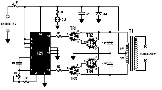
The final power transistors TR2 and TR4 must be mounted on appropriately sized heatsinks to prevent overheating. Suitable options include MJ4033, MJ3007, or other NPN transistors. The maximum power output is dependent on the transformer T1's core size. For...
The AD650 is a voltage-to-frequency (V/F) and frequency-to-voltage (F/V) converter that offers high-frequency operation and low nonlinearity, features that were previously unavailable in a monolithic form. Its inherent monotonicity in the V/F transfer function makes the AD650 suitable for...
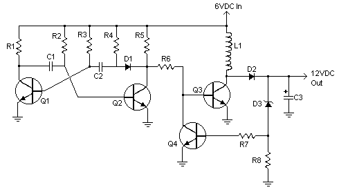
This inverter circuit can provide up to 800mA of 12V power from a 6V supply. For example, you could run 12V car accessories in a 6V car. The circuit is simple, about 75% efficient and quite useful. By changing...