
ASTABLE BLOCKING OSCILLATOR
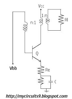
The described circuit operates as a pulse generator utilizing a transistor and a capacitor. Initially, the capacitor C1 holds a voltage greater than the difference between the supply voltage (Vbb) and the base-emitter cutoff voltage (Vg). In this state, the transistor remains off, and C1 discharges through resistor R1, following an exponential decay characterized by the time constant τ = R1C1.
Once the voltage across C1 (V1) decreases to the threshold Vbb - Vg, the transistor begins to conduct. This transition marks the beginning of the regenerative process: the collector current increases, which reduces the collector voltage. The reduction in collector voltage induces an increase in the base voltage through the pulse transformer, leading to a further increase in base current. This positive feedback loop rapidly drives the transistor into saturation, allowing it to generate a pulse.
During the duration of the pulse (tp), capacitor C1 is recharged, and its voltage rises above the initial value. After the pulse ends, the transistor exits saturation and returns to the cutoff state. During this cutoff period, C1 discharges again until the voltage drops to the level that permits the transistor to enter its active region once more. This cyclical process enables the generation of a series of pulses, with the frequency and duty cycle determined by the values of R1, C1, and the characteristics of the pulse transformer and transistor.
The design of this circuit is crucial in applications where pulse generation is needed, such as in oscillators, timing circuits, and switching power supplies. Proper component selection and configuration are essential to ensure reliable operation and desired performance characteristics.Assume initially, that there is a voltage Vc on capacitor C1 larger than Vbb-Vg. Where Vg is the cut in base to Emitter voltage and g represent Gamma. Hence the transistor is off and the capacitor C1 discharges exponentially towards ground with a time constant R1 C1. When V1 becames equal to Vbb-Vg, the base current starts to flow and the transist or comes out of cutoff. The flow of current through collector further lowers the collector voltage and through inductive coupling of pulse Transformer increases the base voltage. This further increases the base current and hence the collector current. This regenerative action quickly brings the transistor in saturation. The pulse is generated and during the pulse duration tp, the capacitor C1 is recharged and attains a voltage V1, which is larger than the value it had at the beginning of the pulse.
The transistor comes out of saturation and the regenerative action brings it in the cutoff. The transistor now remains off for a time tp during which capacitor C1 discharges to the voltage at which transistor Q again enters its active region. At this point the cycle repeats itself. 🔗 External reference
Related Circuits
In a sine wave oscillator circuit, a thermistor and an incandescent lamp are often utilized to stabilize the output of the circuit at a fixed value. The resistance of... The sine wave oscillator circuit is designed to generate a continuous...
The schematic diagram presented is of a twin "T" phase shift oscillator, an audio oscillator. This oscillator derives its name from the phase shift network formed by resistors R3, R4, and capacitors C1, C2, and C3. This network shifts...
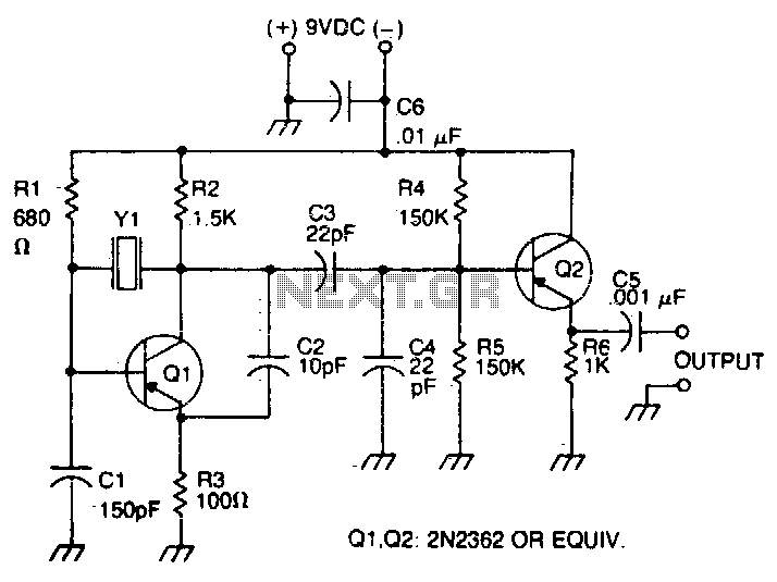
The oscillator transistor is Q1, and the crystal is placed between the collector and base. Feedback is improved by the use of the collector-emitter capacitor C2. Transistor Q2 is used as an output buffer. The circuit described features an oscillator...
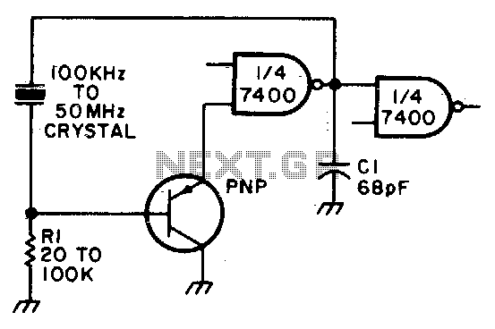
Adjust Rl for approximately 2 volts at the output of the first gate. Additionally, adjust Cl for optimal output. In the context of electronic circuit design, the output voltage of a gate, such as a logic gate or operational amplifier,...
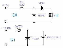
These two circuits are interesting from an academic point of view. Their practical implementation is rather critical and it is not easy to get steady operation. Circuit (a) requires a "cooked" zener: connect it first to a constant current...
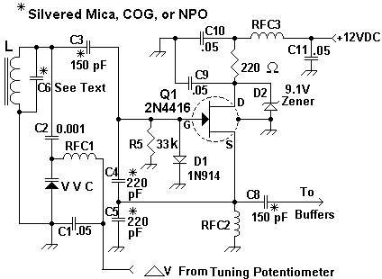
Figure 1 illustrates the VFO oscillator circuit operating within the frequency range of 10.58 to 10.74 MHz. This circuit is a redesigned version of a previously presented Colpitts oscillator, with a clearer representation. The inductor, labeled "L," has an...