
Bipolar transistor biasing

In the design of bipolar transistor amplifiers, achieving a stable Q-point is essential for reliable performance. The biasing network, often composed of resistors, plays a pivotal role in establishing this point. In discrete circuits, simple resistor networks suffice, while integrated circuits may require more sophisticated methods such as current mirrors or bandgap references to ensure stability across varying environmental conditions.
The Q-point's location on the output characteristic curve directly influences the amplifier's linearity and gain. For Class A amplifiers, the Q-point must be carefully set within the active region to prevent distortion when the input signal is applied. Conversely, in digital applications, the Q-point's placement allows for rapid switching between states, optimizing performance for logic-level operations.
Thermal considerations are paramount in amplifier design, as variations in temperature can significantly affect transistor behavior. The negative feedback mechanism is a common solution to counteract thermal runaway, ensuring that increases in current do not lead to further temperature rises. This feedback can be implemented through resistor networks that dynamically adjust the biasing conditions based on the collector current.
The half-voltage principle serves as a practical guideline for biasing, ensuring that the transistor operates within safe limits while maximizing efficiency. By keeping the collector voltage below half of the power supply, the design inherently prevents excessive power dissipation, thereby enhancing reliability.
In summary, the design of bipolar transistor amplifiers necessitates careful consideration of biasing techniques, thermal management, and the stability of the Q-point to ensure optimal performance across various operational conditions. The successful implementation of these principles results in amplifiers that are both efficient and robust, capable of delivering consistent performance in diverse applications.Bipolar transistor amplifiers must be properly biased to operate correctly. In circuits made with individual devices (discrete circuits), biasing networks consisting of resistors are commonly employed. Much more elaborate biasing arrangements are used in integrated circuits, for example, bandgap voltage references and current mirrors.
The operat ing point of a device, also known as bias point, quiescent point, or Q-point, is the point on the output characteristics that shows the DC collector emitter voltage (Vce) and the collector current (Ic) with no input signal applied. The term is normally used in connection with devices such as transistors. For analog operation of a Class A amplifier, the Q-point is placed so the transistor stays in active mode (does not shift to operation in the saturation region or cut-off region) when input is applied.
For digital operation, the Q-point is placed so the transistor does the contrary - switches from the "on" (saturation) to the "off" (cutoff) state. Often, the Q-point is established near the center of the active region of a transistor characteristic to allow similar signal swings in positive and negative directions.
The Q-point should be stable; in particular, it should be insensitive to variations in transistor parameters (for example, should not shift if transistor is replaced by another of the same type), variations in temperature, variations in power supply voltage and so forth. The circuit must also be practical; both easily implemented and cost-effective. At constant current, the voltage across the emitter base junction VBE of a bipolar transistor decreases 2 mV (silicon) and 1.
8mV (germanium) for each 1 °C rise in temperature (reference being 25 °C). By the Ebers Moll model, if the base emitter voltage VBE is held constant and the temperature rises, the current through the base emitter diode IB will increase, and thus the collector current IC will also increase. Depending on the bias point, the power dissipated in the transistor may also increase, which will further increase its temperature and exacerbate the problem.
This deleterious positive feedback results in thermal runaway. [1] There are several approaches to mitigate bipolar transistor thermal runaway. For example, Negative feedback can be built into the biasing circuit so that increased collector current leads to decreased base current. Hence, the increasing collector current throttles its source. The transistor can be biased so that its collector is normally less than half of the power supply voltage, which implies that collector emitter power dissipation is at its maximum value.
Runaway is then impossible because increasing collector current leads to a decrease in dissipated power; this notion is known as the half-voltage principle. This form of biasing is also called base bias. In the example image on the right, the single power source (for example, a battery) is used for both collector and base of a transistor, although separate batteries can also be used.
For a given transistor, Vbe does not vary significantly during use. As Vcc is of fixed value, on selection of RB, the base current IB is fixed. Therefore this type is called fixed bias type of circuit. The common-emitter current gain of a transistor is an important parameter in circuit design, and is specified on the data sheet for a particular transistor. It is denoted as ² on this page. When the transistor is replaced with another one, considerable change in the value of ² can be expected.
Due to this change the operating point will shift. For small-signal transistors (e. g. , not power transistors) with relatively high values of ² (i. e. , between 100 and 200), this configuration will be prone to thermal runaway. In particular, the stability factor, which is a measure of the change in collector current with changes in reverse saturation current, is approximately ²+1. To ensure absolute stability of th 🔗 External reference
Related Circuits
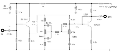
The first BC109C transistor functions as a buffer, delivering a high input impedance of approximately 250k and exhibiting a voltage gain marginally below unity. Given that the Baxendall tone control circuit operates passively, it attenuates all audio frequencies. The...
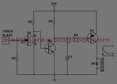
This document describes a series of touch switches that utilize only three transistors. These touch-based transistor switches can activate a load simply by the user touching a metal plate. They are designed to directly switch a relay, enabling operation...
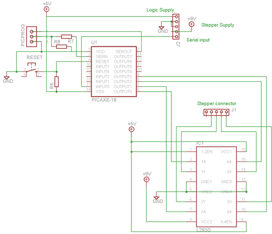
A schematic and program have been developed for operating a bipolar stepper motor through a serial interface, similar to the unipolar configuration. This is significant for the robot arm project, as two of the three stepper motors will be...
This circuit can be adjusted to operate within the frequency range of 87-108 MHz, achieving a transmission distance of approximately 20 to 30 meters. The design incorporates a pair of BC548 transistors, which, while not specifically designated as RF...
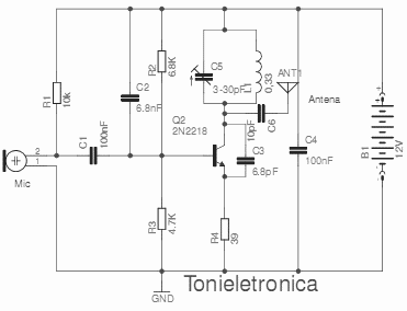
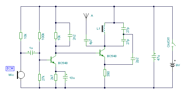
This small transmitter can reach distances of more than 1 km under favorable transmission conditions. Modulation can be achieved using a microphone, such as an electret microphone, or another audio source. The transmitter includes a coil made of 5...

BC517 Bipolar Stepper Motor Control Circuit Diagram. Features: Each winding can carry a positive current. A bipolar motor has two windings. The BC517 bipolar stepper motor control circuit utilizes a BC517 transistor to manage the operation of a bipolar stepper...