
Broadcast Band Rf Amplifier Circuit
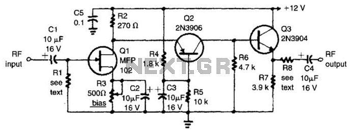
The described circuit is a versatile amplifier design, suitable for a range of applications where signal integrity and stability are critical. The frequency response of 100 Hz to 3 MHz indicates its capability to handle both audio and high-frequency signals, making it ideal for communications and signal processing tasks. The gain of 30 dB is indicative of a moderate amplification level, suitable for boosting weak signals without introducing significant distortion.
The common-source configuration of Q1 allows for high voltage gain and is particularly effective in amplifying low-level signals. The optional resistor R1 provides flexibility in setting the input impedance, which is crucial for matching the circuit to various signal sources. A typical value of 50 ohms is often used to match standard RF components, ensuring maximum power transfer and minimizing signal reflections.
The common-base configuration of Q2 serves a dual purpose: it not only isolates the input from the output but also contributes to the overall stability of the amplifier. This configuration is known for its low input impedance and high output impedance, which is beneficial in applications where signal isolation is necessary.
Q3, as an emitter-follower, is designed to deliver a low output impedance, which is advantageous for driving loads that require current without significant voltage drop. The output impedance of approximately 50 ohms allows for effective interfacing with subsequent stages or external loads.
In scenarios where higher output impedance is desirable, the incorporation of resistor R8 offers a straightforward solution. The relationship defined by the formula Rs ~ ^0lJT - 50 allows for precise control over the output characteristics, enabling the circuit to adapt to varying load requirements.
The option to connect output capacitor C4 directly to the emitter of Q3 provides an alternative output configuration, which may be useful in specific applications where coupling capacitors are required to block DC components while allowing AC signals to pass through.
Overall, this amplifier design combines flexibility, stability, and adaptability, making it suitable for a diverse range of electronic applications. The circuit has a frequency response that ranges from 100 Hz to 3 MHz; the gain is about 30 dB. Field-effect transistor Ql is configured in the common-source self-biased mode; optional resistor R1 allows you to set the input impedance to any desired value. Commonly, it will be 50 . The signal is then direct-coupled to Q2, a common-base circuit that isolates the input and output stages and provides the amplifier`s exceptional stability.
Last, Q3 functions as an emitter-follower, to provide low output impedance (about 50 ). If you need higher output impedance, include resistor R8. It will affect impedance according to this formula: Rs ~ ^0lJT - 50. Otherwise, connect output capacitor C4 directly to the emitter of Q3. 🔗 External reference
Related Circuits
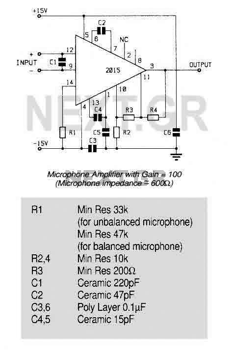
An ultra low noise audio preamplifier particularly suited to microphone preamplification including balanced microphones. The IC features wide bandwidth, low distortion only 0.007% at a gain of 100, and very low noise only 1.3nV/Hz for source impedance up to...
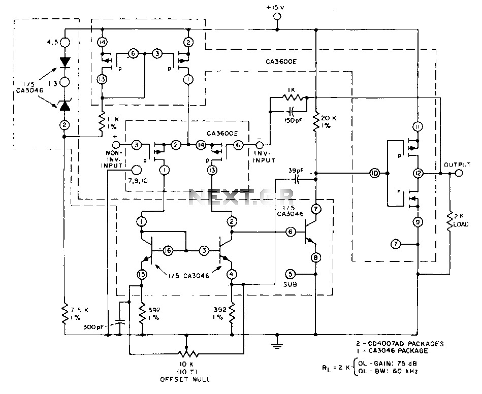
This unity-gain follower amplifier features a CMOS p-channel input, an NPN second-gain stage, and a CMOS inverter output. The integrated circuit components consist of two CA3600E CMOS transistor pairs and a CA3046 NPN transistor array. A zener-regulated leg provides...
CD4060 Timer Circuit 1 minute to 2 hours This is a 1 minute to two-hour timer switch. The 14-stage binary ripple counter Type 4060, IC1, has an... The CD4060 timer circuit is designed to function as a timer switch with...
This transmitter emits an FM signal within the 88 to 108 MHz frequency range, featuring a tone of 19 kHz. This tone can activate the FM MPX pilot carrier indicator, allowing interfacing with external devices. L4 is designed for...
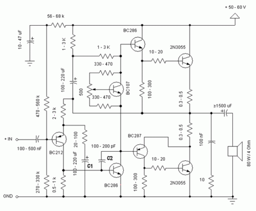
The following circuit illustrates a Power Amplifier Circuit Diagram utilizing a 2N3055 transistor. Features include a 500-ohm current and an optimal voltage of 50V. The power amplifier circuit based on the 2N3055 transistor is designed to deliver significant output power,...
Constantly changing light and sound analog controller circuit 01 The described circuit functions as an analog controller designed to modulate light and sound outputs in a dynamic manner. This circuit typically integrates various electronic components, including resistors, capacitors, transistors, and...
Warning: include(partials/cookie-banner.php): Failed to open stream: Permission denied in /var/www/html/nextgr/view-circuit.php on line 713
Warning: include(): Failed opening 'partials/cookie-banner.php' for inclusion (include_path='.:/usr/share/php') in /var/www/html/nextgr/view-circuit.php on line 713